Equipped with a large-area sample stage compatible with 8-inch wafers.
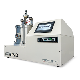
The Magnetron Sputtering Device MSP-8 Inch features a magnetron target electrode and is equipped with a large-area sample stage compatible with 8-inch wafers. The variation in coating thickness is within 10%, effectively utilizing the entire stage area. Coating is done at a voltage of 500V or lower to reduce damage from ion impact. For more details, please contact us or refer to the catalog.

Inquire About This Product
basic information
【Main Features】 - Equipped with a large-area sample stage compatible with 8-inch wafers using a magnetron target electrode. - Coating thickness variation is within 10%, effectively utilizing the entire stage area. - Reduces damage from ion impact with a coating voltage of 500V or less. - Standard target metal is platinum (Pt). - Additional functionality with an ion shower electrode (optional). 【Other Features】 - Achieves a large-area sample stage with a diameter of 200mm using a magnetron target electrode to accommodate larger silicon substrates. - The enlarged sample stage allows for simultaneous coating of 8-inch wafers and multiple SEM samples, improving inspection efficiency. - The magnetron-type electrode forms a magnetic field parallel to the surface of the target metal, trapping electrons generated by plasma discharge in this magnetic field and promoting the plasma formation of the ambient gas. ● For more details, please contact us or refer to the catalog.
Price information
Please contact us.
Price range
P5
Delivery Time
※Please contact us.
Applications/Examples of results
【Usage】 ○ Suitable for high-resolution SEM inspection. ● For more details, please contact us or refer to the catalog.
catalog(1)
Download All Catalogs
Company information

We manufacture sputtering devices, deposition devices, plasma irradiation devices, CVD devices, and vacuum components. We offer a lineup of pre-treatment devices for electron microscope sample preparation and small vacuum devices for research and development institutions. We believe it is our company's mission to quickly and affordably supply the necessary equipment development for those active in cutting-edge technology research and development, and to support development by making incremental improvements and modifications during the experimental process. We are involved in the development, commercialization, sales, and service of experimental instruments and devices necessary for new technology development in the fields of semiconductors, biotechnology, environment, and nanotechnology, as well as devices related to electron microscope sample preparation as cutting-edge analytical tools for new technology development.