Thin film surface treatment processing | Improvement of mold release properties for stamping dies and reduction of takt time.
[Contract Coating Processing] Unique surface treatment technology that can improve the release properties of 'molds' for optical components! Sample testing available.
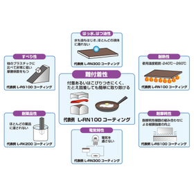
The organic nano-thin film treatment technology "NANOS" can apply functional films that enhance water repellency, oil repellency, dirt resistance (fingerprint resistance), and slipperiness (dynamic friction coefficient) to metal and glass substrates such as stainless steel (SUS) and nickel (Ni) through spray treatment and vacuum deposition using a special fluoropolymer. The maximum temperature of the entire process is 80°C, which minimizes thermal impact on the substrate, and since it is colorless and transparent, it has little effect on optical properties. 【Examples of Adoption】 ■ Target: Stamping molds ■ Purpose: Improved release properties, reduced tact time 【Features】 ○ Excellent water and oil repellency Pure water: over 110°; n-hexadecane: over 68° ○ Thin film thickness can be controlled Spray treatment: 5–10nm (can be controlled in 1nm increments) Vacuum deposition: 5–45nm (can be controlled in 5nm increments) ○ Minimal impact on optical properties (colorless and transparent) ○ Low-temperature process Our surface treatment methods include both deposition and spray methods. You can specify the treatment method or leave it to us. Please feel free to consult with us! (Sales of the machinery itself are subject to consultation.)

Inquire About This Product
basic information
**[Adoption Results and Effects]** **[Spray Method]** ○ Contact glass for scanners → Prevention of dirt adhesion, improved maintenance ○ Optical components (lenses, cover glass, etc.) → Water repellency, prevention of dirt (fingerprint resistance) adhesion ○ Touch panels → Prevention of dirt (fingerprint resistance) adhesion ○ Metal masks for solder printing → Improved printability, reduced maintenance **[Vacuum Deposition Method]** ○ Inkjet heads → Improved printability ○ Molds for optical components → Improved release properties ○ Stamping molds → Improved release properties, reduced tact time ○ Molds for nanoimprinting → Improved release properties, high conformity to fine shapes ○ Jigs for transfer processes (such as gravure) → Improved transferability (release agent-free) ○ Photomasks → Prevention of resist adhesion ○ Probes for AFM and STM → Prevention of foreign substance adhesion ● For more details, please contact us or download the catalog.
Price information
Please contact us.
Delivery Time
※Please contact us.
Applications/Examples of results
For more details, please contact us or download the catalog.
catalog(1)
Download All Catalogs
Company information

Katsurayama Technology Co., Ltd.'s proprietary technology, "NANOS," for organic thin film treatment forms a nano-order thin film on the surfaces of materials such as glass and metal, modifying the surface properties to impart new functions such as water and oil repellency. It is already being used in various fields both domestically and internationally, including mobile phones, smartphones, digital cameras, printers, copiers, LCDs, LEDs, and semiconductor-related applications. We will continue to advance application development and proprietary technology development to support technological innovation in the era of nanotechnology.


![[Case Study] Fluororesin Coating in Such Places](https://image.mono.ipros.com/public/product/image/33a/2000428318/IPROS08939554748196958500.jpeg?w=280&h=280)