Telecentric fθ lens specifications for laser exposure equipment
Telecentric fθ laser exposure device
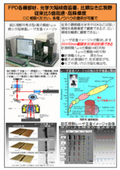
High-precision beam shape rendering is possible across the entire scanning width with telecentric fθ lenses and polygon mirrors using "raster scan type laser exposure."
This is a "laser exposure machine" that directly exposes positive and negative resists without a mask for pattern formation of insulating films, metal patterns, and the formation of banks and partitions in MEMS shapes related to printed electronics. It enables high-precision beam shape drawing across the entire scanning width through "raster scan type laser exposure" using a telecentric fθ lens and a polygon mirror. Laser wavelengths such as 375, 405, 650, 780, and 830 nm, including h-line and i-line, are selectable. Laser spot diameters of 2 μm (@405 nm), 10 μm, 22 μm, 30 μm, etc. Resolution options include up to 25,400 dpi, 5,080 dpi, and 3,000 dpi, among others. It can accommodate a wide range of photosensitive resists, including various semiconductor exposure resists, polyimide resists, and photosensitive Ag. Electrode formation can be achieved using organic TFT gate insulating films, photosensitive Ag inks, etc. Creating complex pattern shapes that are difficult with inkjet, flexo, or screen methods is made easy.

Inquire About This Product
basic information
Due to laser exposure using a telecentric fθ lens, it is possible to achieve high-precision drawing with the same beam shape across the entire scanning width. The main body of the direct drawing device has been compactly designed, making it ideal for high-resolution exposure of small lots with a variety of products in a space-saving manner. [Basic Specifications] Custom options are available for scanning widths other than those listed below (telecentric fθ lens) Model: LSU-1002, LSU-6010, LSU-12522, LSU-25030 Laser Wavelength: 375, 405, 650, 780, 830 nm; 355, 488, 532 nm Laser Spot Diameter (at laser wavelength 405 nm): 2 μm, 10 μm, 22 μm, 30 μm Laser Scanning Width: 10 mm, 60 mm, 125 mm, 250 mm Data Resolution: up to 25,400 dpi, up to 5,080 dpi, up to 3,000 dpi, up to 1,500 dpi Data Format: Bitmap (BMP) Focus Unit (manual operation): Z stage [Optional Features] Focus confirmation unit, repeated exposure function, reference hole position adjustment function, air chuck table.
Price information
Please feel free to contact us.
Price range
P7
Delivery Time
Applications/Examples of results
This is a device that achieves maskless pattern formation related to printed electronics. It is a "laser exposure machine" that directly exposes positive and negative resists for pattern formation of insulating films, metal pattern formation, and the formation of MEMS shapes such as banks and partitions without a mask. It can also accommodate wavelengths such as h-line and i-line. With a telecentric fθ lens and a polygon mirror, it enables high-precision beam shape drawing across the entire scanning width using "raster scan-type laser exposure." Laser wavelengths including h-line and i-line, such as 375, 405, 650, 780, and 830 nm, are selectable. Laser spot diameters of 2 μm (@405 nm), 10 μm, 22 μm, 30 μm, etc. Resolution options include up to 25,400 dpi, 5,080 dpi, 3,000 dpi, etc.
catalog(2)
Download All Catalogs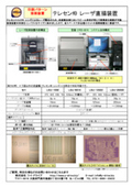
Company information

Y-Drive Co., Ltd. is a company that develops and researches printed electronics technology. In addition to the production of electronic devices using inkjet methods, micro-nano molding methods, and printing methods, we also undertake the fabrication of fine 2D and 3D printed wiring/structures (fabrication of structures at scales below a few micrometers) and the development of various electronic circuit boards. We also accept contracts for various image processing software (camera systems and 3D sensor systems), FPGA design, electronic control software development, and embedded electronic device development.
![[Problem Solving] Improving Cut Surface Quality Expanding Work Range with Fiber Laser Processing Machine](https://image.mono.ipros.com/public/product/image/e0c/2001140843/IPROS9483816829010595099.jpg?w=280&h=280)


![[Now accepting applications for actual machine demonstrations] Laser Marker](https://image.mono.ipros.com/public/product/image/76d/2000569890/IPROS06395382160466634803.png?w=280&h=280)


