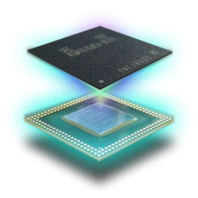
3D implementation contributes to miniaturization and high density.
PoP technology is adopted in products that require miniaturization and high density, such as smartphones and digital still cameras, and our company has achieved a cumulative production record of over 100 million units to date.
In addition to PoP, we also possess technology for stacking substrates to accommodate product miniaturization.
【Features】
■ By stacking two semiconductor packages, it is possible to reduce the footprint on the substrate.
■ By using wiring between the upper and lower packages, we can shorten the wiring length compared to wiring on the substrate, enabling high-speed wiring.
■ By using tested packages that are quality assured, we can reduce the failure rate compared to SiP.
■ In addition to PoP, we can also accommodate substrate stacking.
Inquiry about this news
Contact Us OnlineMore Details & Registration
Details & Registration
Related Links
Related product

Related catalog(1)
![POP PreStack Technology [Mass Production Contract]](https://image.mono.ipros.com/public/catalog/image/01/744/566360/IPROS93285532248840387422.jpeg?w=120&h=170)
Distributors


