We contribute to miniaturization of products through 3D implementation technologies such as PoP (Package on Package) implementation.
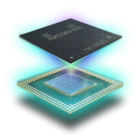
PoP technology is adopted in products that require miniaturization and high density, such as smartphones and digital still cameras, and our company has achieved a cumulative production record of over 100 million units to date. Additionally, we possess technologies for stacking substrates beyond PoP, enabling us to respond to product miniaturization. 【Features】 ■ By stacking two semiconductor packages, it is possible to reduce the footprint on the substrate. ■ By using wiring between the upper and lower packages, we can shorten the wiring length compared to wiring on the substrate, enabling high-speed wiring. ■ By using tested packages with guaranteed quality, we can reduce the failure rate compared to SiP. ■ We can also accommodate substrate stacking beyond PoP. *For more details, please refer to the PDF document or feel free to contact us.

Inquire About This Product
basic information
For more details, please refer to the PDF document or feel free to contact us.
Price range
Delivery Time
Applications/Examples of results
For more details, please refer to the PDF document or feel free to contact us.
catalog(1)
Download All Catalogs![POP PreStack Technology [Mass Production Contract]](https://image.mono.ipros.com/public/catalog/image/01/744/566360/IPROS93285532248840387422.jpeg?w=120&h=170)
News about this product(1)
Company information

Our company was established in April 2016 as a company that consistently handles various functions of manufacturing, including the development of core technologies, product design, production technology and manufacturing, parts procurement, logistics, and repair services. Based on the know-how, skills, and insights we have accumulated in the "manufacturing" of Sony products, we provide attractive products and services with high quality that our customers can trust. Every day, we receive various requests and consultations from customers in different industries, and our "team of manufacturing professionals" responds to even the most challenging demands with enthusiasm.
![[Data] WTI Blog April 2018 - March 2019](https://image.mono.ipros.com/public/product/image/419/2000565478/IPROS98269808061488054847.jpeg?w=280&h=280)
![[Information] WTI Blog: Semiconductor Packaging Edition](https://image.mono.ipros.com/public/product/image/f15/2000641055/IPROS33294883006593077590.jpeg?w=280&h=280)
![[Data] WTI Blog January 2022](https://image.mono.ipros.com/public/product/image/2e9/2000686771/IPROS86311445361732062134.jpeg?w=280&h=280)


