[Laser Micromachining Examples] Polyimide, Ultra-Fine Hole Machining, and Hole Machining Examples on Stainless Steel
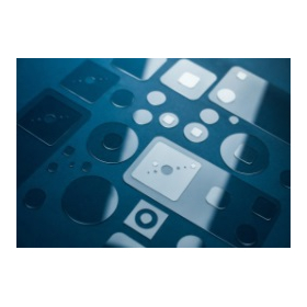
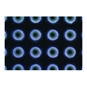
Here are three examples of micro hole processing! You can also view processing photos from the left. ■ Hole processing of polyimide This is the laser emission side in the left photo. The reverse taper (the hole diameter on the emission side is larger than that on the incident side) is controlled at 13°. Positioning accuracy of ±250 nm and repeatability of ±250 nm have been achieved. ■ Ultra-fine hole processing A hole of approximately Φ10 µm was processed using a laser on a metal plate with a thickness of 100 µm. There is no thermal impact, resulting in a very clean round hole. Such high aspect ratio laser microprocessing is also possible. ■ Hole processing on stainless steel This is hole processing on 100 µm thick stainless steel SUS430. A fine hole with a diameter of Φ35 µm can be processed using a laser. It is also possible to create a mesh structure with multi-hole processing without distortion due to heat. For more details on various examples of laser processing, please download and view "Laser Microprocessing Machine Introduction & Problem Solving Case Collection Vol. 1" from the link below.

Inquire About This Product
basic information
Hikari Co., Ltd. is a joint venture with Germany's 3D-Micromac, a world-class manufacturer of laser microprocessing equipment, and acts as the general agent in Japan. The company has introduced pico-second laser microprocessing equipment manufactured by them, achieving high-quality processing for drilling, cutting, and marking on various materials with this state-of-the-art laser microprocessing equipment. *For detailed information on equipment introduction and processing case studies, please download and view the brochure.*
Price range
Delivery Time
Applications/Examples of results
【Medical and Life Sciences Field】 Various markings, medical stent processing, thrombus filter processing, microchannel formation, ophthalmic treatment, injection needle processing, leak test holes, biochip mold processing, laser scalpel, protein crystallization, hollow micro-needles, etc. 【Solar Cell Field】 Through-hole processing, edge isolation, P1, P2, P3 scribing, marking, wafer dicing, organic material coating, drying furnace, texturing, device cutting, laser welding. 【Electrical and Electronic Field】 Through-hole processing, wafer cutting, insulation processing/trimming, marking, pinhole processing, electrode formation, metal mask processing, lens cutting, 3D printing, device cutting, texturing, internal glass marking. 【Precision Instruments Field】 Optical waveguide processing, fine mold processing, watch parts processing, microchannel formation, inkjet nozzle processing, resin parts cutting, surface roughness control, fine welding, gear processing, electrode processing, fine marking, fine nozzle processing. For more details on our introduction and processing achievements, please download the brochure or contact us directly.
catalog(1)
Download All Catalogs
Company information

We are a joint venture with Germany's 3D-Micromac, a world-class manufacturer of laser microfabrication equipment, and we operate as the general agent in Japan. Microfabrication equipment using picosecond and femtosecond lasers is widely applied in the production of thin-film solar cells, organic EL for lighting, automotive parts, precision machine components, cutting and drilling of transparent materials with internal marking, and medical devices. Additionally, high-precision inkjet nozzle micro-drilling equipment using excimer lasers is also adopted by world-class inkjet manufacturers. We strive to meet our customers' advanced microfabrication requirements and contribute to the technological innovation of Japan's manufacturing industry.

![[Prototype Acceptance in Progress] Examples of Laser Microfabrication Applications](https://image.mono.ipros.com/public/product/image/e60/2000156206/IPROS6108904142426905709.jpg?w=280&h=280)