In a multilayer substrate, it is possible to obtain information for each layer! By using a length measurement tool, you can measure the length.
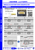
The biggest advantage of angled CT is that it allows for non-destructive CT observation. It is suitable for obtaining planar information and can provide information for each layer in a multilayer substrate. Additionally, by using a length measurement tool, it is also possible to measure lengths. In our measurements, we observed a difference of about 7-14% compared to the results from optical microscope images, but it seems effective for those who want to understand internal structures non-destructively. Please feel free to contact us when needed. 【Features】 ■ Non-destructive CT observation ■ Suitable for obtaining planar information ■ Capable of obtaining information for each layer in multilayer substrates *For more details, please refer to the PDF document or feel free to contact us.

Inquire About This Product
basic information
Observation Case of Laminated Substrate (Oblique CT Observation) ■ With Cheetah EVO, it is possible to perform CT observation on samples with minimal surface irregularities and approximately 200mm in size without causing damage. ■ Through X-ray transmission observation, it is possible to confirm the patterns of each layer by acquiring images using oblique CT. ■ Length measurements can also be made using a measurement tool. ■ The measurement results showed a difference of about 7-14% compared to the results from optical microscope images, but it is effective for cases where one wants to understand the internal structure non-destructively. *For more details, please refer to the PDF document or feel free to contact us.
Price range
Delivery Time
Applications/Examples of results
For more details, please refer to the PDF document or feel free to contact us.
catalog(16)
Download All Catalogs

![[Cheetah EVO Case Study] Observation of Inductor Coils (Orthogonal CT Observation)](https://image.mono.ipros.com/public/catalog/image/01/d94/478426/IPROS11705774122712488334.jpeg?w=120&h=170)
![[Cheetah EVO Case Study] Observation of IC Type Coils](https://image.mono.ipros.com/public/catalog/image/01/40e/478427/IPROS43080621970966399269.jpeg?w=120&h=170)


![[X-ray fluoroscopy and CT examination equipment] Examples of combined use of transmission observation and image processing technology.](https://image.mono.ipros.com/public/catalog/image/01/ce8/508354/IPROS20790474618652315106.jpeg?w=120&h=170)

![[Case Study] X-ray Fluoroscopy and CT Examination Equipment](https://image.mono.ipros.com/public/catalog/image/01/779/511806/IPROS69821420652988785136.jpeg?w=120&h=170)
![[Defective Analysis Case] X-ray Observation of AC Adapter](https://image.mono.ipros.com/public/catalog/image/01/409/549849/IPROS70295238176529335250.jpeg?w=120&h=170)
![[Observation Case] X-ray Observation of a Toggle Switch](https://image.mono.ipros.com/public/catalog/image/01/9cc/549975/IPROS28998578668948308132.jpeg?w=120&h=170)

Company information

Aites was established in 1993, originating from the quality assurance department of the IBM Japan Yasu office. Based on the technical expertise cultivated through cutting-edge defect analysis and reliability assurance of electronic components at the IBM Japan Yasu office, we have provided various products and services that support the development and manufacturing of semiconductors, displays, organic EL, solar cells, and electronic components to customers both domestically and internationally.


