What is the semiconductor manufacturing process? An introduction to surface treatment that supports semiconductor manufacturing.
What is the semiconductor manufacturing process? This introduces the surface treatments used in semiconductor manufacturing equipment.
The semiconductor manufacturing process refers to a series of steps involved in designing, producing, and shipping semiconductor devices. Semiconductor devices are essential components used in various modern electronic devices such as computers, smartphones, automotive electronics, and LEDs. The semiconductor manufacturing process requires high purity and precision technology, and is often conducted in automated clean rooms. 1. Design → Photomask production Logic circuit design, layout design, photomask production 2. Front-end process (wafer processing) Procurement of silicon wafers → Cleaning → Film deposition → Photolithography → Ion implantation → Wiring → Inspection 3. Back-end process (assembly) Dicing → Die bonding → Wire bonding → Encapsulation → Solder ball mounting → Separation → Stamping → Inspection → Packaging and shipping In the semiconductor manufacturing process, especially in the front-end process, a high level of precision at the nano level is required, necessitating high purity and precision. Surface treatments, including fluororesin coating, support semiconductor manufacturing and play a significant role in semiconductor manufacturing equipment, an area in which Japan excels. Below, we will introduce surface treatments that are indispensable in semiconductor manufacturing.

Inquire About This Product
Related Videos
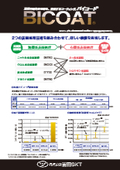
basic information
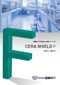
■Applications such as semiconductor manufacturing lines - Selected surface treatment 'TEFLON (TM) fluoropolymer coating' ■Applications such as wafer and glass handling - Selected surface treatment 'SAFELON (R)' 'PBI, PI coating' ■Applications such as precision nozzles, MEMS components, and optical lenses - Selected surface treatment 'NANOPROCESS (R)' ■Applications such as chemical supply tanks - Selected surface treatment 'TEFLON (TM) fluoropolymer coating' 'SAFELON (R) AP+' 'MY LINING (R)' ■Applications such as clean room walls, laboratory equipment, and various tools - Selected surface treatment 'SERASHIELD F' ■Applications for high-temperature equipment components (rolls, heater covers) - Selected surface treatment 'SGN coating' *You can download the PDF of the introduced surface treatment products. For detailed information about the products, please visit the "Yoshida SKT official website."*
Price range
Delivery Time
Applications/Examples of results
For more details, please contact us or visit the "Yoshida SKT Official Website."
catalog(10)
Download All Catalogs


News about this product(1)

Company information

To maximize the performance of manufacturing equipment and machine parts, Yoshida SKT derives the "optimal solution" tailored to our customers from hundreds of surface treatment technologies. - Decreased productivity due to adhesive troubles - Instability in product quality due to friction - Early deterioration of equipment due to corrosion We respond to these challenges in the manufacturing field with our extensive track record and reliable technical expertise. In 1963, we began fluoropolymer processing. In 1968, we signed a licensing agreement with DuPont (now Chemours), supporting manufacturing innovations for over 2,000 customers across various industries, from automotive to medical and aerospace. Furthermore, in 2024, we are focusing on the development of next-generation products, such as PFAS-free coatings, contributing to the advancement of sustainable manufacturing. With a three-base system in Nagoya, Tokyo, and Yamaguchi, we flexibly respond to both mass production and custom orders. Our consistent quality management system ensures that we deliver reliable quality. For solving challenges in the manufacturing field, trust the surface treatment experts at Yoshida SKT.


![[Coating Example] Food Machinery Parts (PTFE・PFA)](https://image.mono.ipros.com/public/product/image/8e0/2000493614/IPROS81896690695890946835.jpeg?w=280&h=280)


