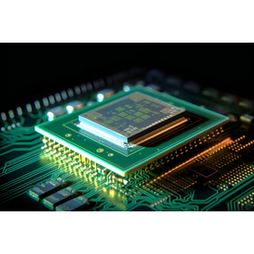
3D circuit board (MID wiring) / substrate with embedded electronic components
3D circuit board MID wiring (Molded Interconnect Device) embedded electronic component board
3D circuit board [MID wiring (Molded Interconnect Device)] / substrate with embedded electronic components
Our company provides contract design and development of electronic devices (ODM) as well as contract manufacturing services for electronic devices (EMS). We are involved not only in the design and manufacturing of flexible printed circuits but also in circuit design, structural design, software development, cable and harness production, and we collaborate with product development personnel from the planning stage to bring products to market. Various industries are advancing in miniaturization and weight reduction. To differentiate ourselves from competitors while considering mass production efficiency, we propose a wide range of solutions, not limited to flexible printed circuits, including 3D-MID wiring cases with conductor formation on resin housing surfaces and embedded substrates that incorporate electronic components into printed circuit boards. Etching, plating, vacuum deposition, EB deposition, sputtering, thin film formation, photolithography, ion plating, thermal CVD, plasma CVD, dry etching, film ITO, film metal patterning, fine patterns, WLP, silicon wafers, RDL, bump formation, TEG, dry etching, wet etching, MEMS, organic EL, metallization, glass etching, semi-additive etching, transparent resist, transparency, high heat-resistant resin.
Inquire About This Product
basic information
Etching, plating, vacuum deposition, EB deposition, sputtering, thin film formation, photolithography, ion plating, thermal CVD, plasma CVD, dry etching, film ITO, film metal patterning, polyamide (PA), polycarbonate (PC), polyoxymethylene (POM), modified polyphenylene ether (m-PPE), polybutylene terephthalate (PBT), GF reinforced polyethylene terephthalate (GE-PET), ultra-high molecular weight polyethylene (UHPE), polyphenylene sulfide (PPS), polyarylate (PAR), polysulfone (PSU), polyether sulfone (PES), polyether ether ketone (PEEK), polyether imide (PEI), polyamide imide (PAI), liquid crystal polymer (LCP), polyimide (PI), polyarylate (PAR), polysulfone (PSF), polytetrafluoroethylene (PTFE) fluoropolymer, thermoplastic elastomer, polymethylpentene (PMP), biodegradable plastic (bioplastic), cellulose-based plastic, urethane, nylon, powder molding, casting, light curing, nylon molding, resin cutting.
Price information
Etching, plating, vacuum deposition, EB deposition, sputtering, thin film formation, photolithography, ion plating, thermal CVD, plasma CVD, dry etching, film ITO, film metal patterning, fine pattern, WLP, silicon wafer, RDL, bump formation, TEG, dry etching, wet etching, MEMS, organic EL, metallization, glass etching, semi-additive, printed circuit board, flexible substrate, FPC, flexible substrate, plating, solder, narrow pitch.
Delivery Time
Applications/Examples of results
Etching, plating, vacuum deposition, EB deposition, sputtering, thin film formation, photolithography, ion plating, thermal CVD, plasma CVD, dry etching, film ITO, film metal patterning, fine pattern, WLP, silicon wafer, RDL, bump formation, TEG, dry etching, wet etching, MEMS, organic EL, metallization, glass etching, semi-additive, printed circuit board, flexible substrate, FPC, flexible substrate, plating, solder, narrow pitch, transparent flexible, transparent resist, transparent, high heat-resistant resin, polyamide (PA), polycarbonate (PC), polyacetal (POM), modified polyphenylene ether (m-PPE), polybutylene terephthalate (PBT), GF reinforced polyethylene terephthalate (GE-PET), ultra-high molecular weight polyethylene (UHPE), polyphenylene sulfide (PPS), polyarylate (PAR), polysulfone (PSU), polyether sulfone (PES), polyether ether ketone (PEEK), powder molding, casting, light molding, nylon molding.
Company information
Sartec is a manufacturing support company based in Hamamatsu City, Shizuoka Prefecture, focused on flexible circuit board design. Going beyond our core strength and origin in "flexible circuit board design," we provide support tailored to each stage of development, from initial development to mass production, including software/hardware development, enclosure design, prototype evaluation, and manufacturing support. Printed circuit boards are an essential component often referred to as the "heart" of a product. Because we have a deep understanding of this core part, we can create a development process with minimal setbacks through our approach of "manufacturing that considers the user's experience" combined with "process design capabilities that encompass the entire product," turning the ideals of researchers and developers into tangible reality. At Sartec, we have a wide range of achievements across various fields, from cutting-edge special designs in medical and aerospace sectors to everyday products like automobiles and IoT appliances. We are also flexibly responding to the semiconductor field, which has been gaining attention in recent years, expanding the possibilities of technology through processes like film formation. If you have a desire to challenge conventional industry norms and pursue products or new technologies that do not yet exist in the world, please feel free to consult with Sartec.
![[Component Assembly and Various Manufacturing] Flexible Circuit Boards, FPC, Flexible Boards](https://image.mono.ipros.com/public/product/image/308/2000509612/IPROS45740238299848604956.jpeg?w=280&h=280)


![[Exhibition Report] We exhibited at NEPCON Japan 2026!](https://image.mono.ipros.com/public/default/object/noimage_l.gif?w=280&h=280)
