Leave the evaluation of contact surface/interface thermal resistance of semiconductor devices to us.
Thermal microscope, thermo-wave analyzer, request measurement using steady-state thermal conductivity measurement device.
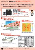
Precision multi-scale thermal resistance evaluation technology to solve contact surface/interface thermal issues in semiconductor device packaging.
With the advancement of semiconductor devices, the thermal resistance of contact surfaces and interfaces has become an important issue. In AI chips, GPUs, NPUs, and power semiconductors, the amount of heat generated has been increasing year by year, and even small thermal resistances can lead to serious temperature rises. Furthermore, in advanced packaging technologies such as flip-chip mounting and heterogeneous integration, controlling the thermal resistance at the bonding interface is essential. There is also a demand for the development of higher-performance materials and precise thermal property evaluations for solder joints in conventional technologies, as well as TIM1 inside the package and TIM2 outside. Bethel's product line enables diverse thermal resistance evaluations on scales from micrometers to several tens of millimeters through thermal microscopes (TM), thermo-wave analyzers (TA), and steady-state thermal conductivity measurement devices (SS-H40).

Inquire About This Product
basic information
Measurable sizes: Thermal microscope: 1μm to 200μm Thermal wave analyzer: 10μm to 2mm Steady-state thermal conductivity measurement device: 100μm to 20mm
Price information
Requested measurement prices: Thermal microscope: 180,000 yen and up Thermowave analyzer: 80,000 yen and up Steady-state thermal conductivity measurement device: 20,000 yen and up *Prices vary depending on the measurement content. Please contact us or visit the URL below. https://hrd-thermal.jp/measurement/value/
Price range
P4
Delivery Time
P4
※We can usually respond within 2 to 3 weeks. Urgent requests are also possible. Please contact us.
Applications/Examples of results
Usage examples: - Measure the difference in thermal conductivity in the thickness direction and in-plane direction. - Measure the difference in thermal conductivity at different locations. (TA35) - Measure thermal conductivity by changing the temperature. (Optional) - Measure thin materials with high thermal conductivity. - Measure thermal conductivity for the development of heat dissipation materials. *Not only measurement requests but also equipment sales are possible. Examples of measurement targets: - Semiconductor materials (Si, SiC, GaN, GaO, diamond, etc.) - Electronic substrate circuit materials (glass epoxy, polyimide sheets, various metals, AlN, SiC, etc.) - Heat dissipation materials (graphite sheets, aluminum, copper, diamond, etc.) - Composite materials (GFRP, CFRP, high thermal conductivity resins, etc.) - Various TIMs (thermal pads, thermal conductive grease, PCM, etc.) - Various coatings (insulating films, heat-resistant coatings, oxidation-resistant coatings, metal films, etc.)
Line up(3)
| Model number | overview |
|---|---|
| Thermal Microscope | Suitable for evaluating interfacial thermal resistance at micro sizes |
| Thermo Wave Analyzer | Suitable for evaluating interfacial thermal resistance of solder, sintered materials, etc. |
| Steady-State Thermal Conductivity Measurement Device | Suitable for evaluating contact thermal resistance of TIM, thermal conductive grease, adhesives, metal surfaces, etc. |
catalog(17)
Download All Catalogs


![[Technical Data] Measurement Principles and Equipment for Thermal Diffusivity and Thermal Conductivity of Thermowave Analyzers](https://image.mono.ipros.com/public/catalog/image/01/ff8/760064/IPROS37439171752331508250.jpeg?w=120&h=170)
![[Technical Data] Measurement Examples of Thermal Diffusivity and Thermal Conductivity of Thermal Interface Materials Using a ThermoWave Analyzer](https://image.mono.ipros.com/public/catalog/image/01/654/760065/IPROS61913308382735953441.jpeg?w=120&h=170)


![[Technical Data] Measurement Principles and Equipment for Thermal Penetration Rate and Thermal Conductivity of Thermal Microscopes](https://image.mono.ipros.com/public/catalog/image/01/09b/760078/IPROS01930383624445469439.jpeg?w=120&h=170)
![[Information] Manga "Heat Warrior Thermoman"](https://image.mono.ipros.com/public/catalog/image/01/21c/760079/IPROS57242822436348474358.jpeg?w=120&h=170)

Company information

Leveraging the assembly technology cultivated over many years, we have expanded our business areas to include the development of precision component assembly, thermal property measurement devices, contract measurement services, and the development of medical and dental plastic products equipped with clean rooms. We deepen and integrate our "original products" from a unique manufacturing perspective, consolidating our know-how and technology. With "speedy decision-making and execution," which is a strength unique to Bethel, we provide high-quality products under the "Made by BETHEL" label. Our wish at Bethel is for our customers who use Bethel products to be satisfied with our products, manufacturing, and services, and to feel that they made the right choice in trusting our company. Furthermore, we hope that the satisfaction of our customers will lead to the happiness of each employee who works here.


![[Proposal for Evaluation Device] Inverter Characteristic Testing Device](https://image.mono.ipros.com/public/product/image/f8f/2000438216/IPROS23028065678282755360.jpeg?w=280&h=280)
![Manual Sample Grinder "IM-P2" [Made in Japan]](https://image.mono.ipros.com/public/product/image/0cc/2000250216/IPROS11647652581559110087.png?w=280&h=280)


![[Patent] Achieving an air nozzle that completely removes water with air blow.](https://image.mono.ipros.com/public/product/image/2116982/IPROS16998950562973190030.png?w=280&h=280)