Identification of defect locations and overall understanding by PL enables detailed observation of defect areas using TEM!
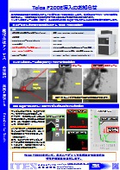
I would like to introduce "TEM observation of PL emission sites in SiC." The basal plane dislocations (BPD) present in SiC substrates are known to amplify defects during forward bias, degrading device characteristics. In this study, we identified small BPDs using photoluminescence (PL) and observed the emission sites with TEM. By identifying defect locations and obtaining an overall view through PL, detailed observation of the defect areas with TEM becomes possible. For more details, please refer to the materials provided. 【Device Overview (Partial)】 ■ PL (Photoluminescence) ■ Equipment used: In-house PL imaging device ■ Excitation light: Ultra-high pressure mercury lamp UV light source (285–350nm) ■ The observation wavelength can be selected based on the type of defects to be captured. *For more information, please download the PDF or feel free to contact us.

Inquire About This Product
basic information
【Overview of Other Equipment】 ■TEM (Transmission Electron Microscope) ■Equipment Used: JEOL JEM-4000FX ■Accelerating Voltage: 400kV ■Electrons accelerated at high voltage are irradiated onto the sample, and the transmitted electrons are imaged to obtain an enlarged image. ■By utilizing unique positioning technology, it is possible to visualize extremely small objects that cannot be recognized in optical images with a high probability using SEM and TEM. *For more details, please download the PDF or feel free to contact us.
Price range
Delivery Time
Applications/Examples of results
For more details, please download the PDF or feel free to contact us.
catalog(14)
Download All Catalogs


Company information

Aites was established in 1993, originating from the quality assurance department of the IBM Japan Yasu office. Based on the technical expertise cultivated through cutting-edge defect analysis and reliability assurance of electronic components at the IBM Japan Yasu office, we have provided various products and services that support the development and manufacturing of semiconductors, displays, organic EL, solar cells, and electronic components to customers both domestically and internationally.


