We have compiled a list of manufacturers, distributors, product information, reference prices, and rankings for パッド印刷微細印刷技術.
ipros is IPROS GMS IPROS One of the largest technical database sites in Japan that collects information on.

パッド印刷微細印刷技術 - List of Manufacturers, Suppliers, Companies and Products | IPROS GMS

パッド印刷微細印刷技術 Product List

1~4 item / All 4 items

Displayed results

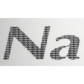
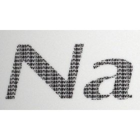
Fine printing technology for pad printing in communication equipment.

The serial number of the communication device is also clear. Challenging the limits of PAD printing.

In the telecommunications equipment industry, there is a demand for the printing of small yet highly visible serial numbers for product identification and tracking. This is particularly important for devices that are becoming smaller, where accurate and clear printing in limited space is crucial. Blurry printing can lead to miscommunication and management confusion. Our pad printing technology achieves fine line printing at 0.04mm, addressing the challenges of serial number printing in telecommunications equipment. 【Application Scenarios】 - Serial number printing on small electronic devices - Fine text printing on nameplates - Ensuring product traceability 【Benefits of Implementation】 - Accurate information transmission due to high visibility - Meeting printing needs in limited spaces - Improvement in product quality and reliability

  • 2305?.jpg
  • 260626_インコ.png
  • Printing Machinery
  • パッド印刷微細印刷技術

Added to bookmarks

Bookmarks list

Bookmark has been removed

Bookmarks list

You can't add any more bookmarks

By registering as a member, you can increase the number of bookmarks you can save and organize them with labels.

Free membership registration

Fine printing technology for pad printing of optical lenses.

Support for printing fine coating information on optical lenses.

In the optical lens industry, it is essential to accurately and clearly display coating information that indicates the performance and quality of products on the lens surface. Particularly, conveying information in fine text and symbols is crucial for communicating necessary information without compromising the visibility and design of the lens. Blurry printing can lead to a decrease in product reliability and customer satisfaction. Our pad printing technology achieves fine line printing of 0.04mm and contributes to the printing of detailed coating information on optical lenses with a plate-making accuracy of ±0.01mm. 【Application Scenarios】 - Printing fine logos and model numbers on the lens surface - Identification display of coating specifications - Precise marking that does not compromise design quality 【Benefits of Implementation】 - Improved product identification - Strengthened quality control - Balancing design quality and functionality

  • 2305?.jpg
  • 260626_インコ.png
  • Printing Machinery
  • パッド印刷微細印刷技術

Added to bookmarks

Bookmarks list

Bookmark has been removed

Bookmarks list

You can't add any more bookmarks

By registering as a member, you can increase the number of bookmarks you can save and organize them with labels.

Free membership registration

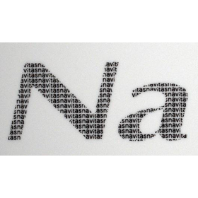
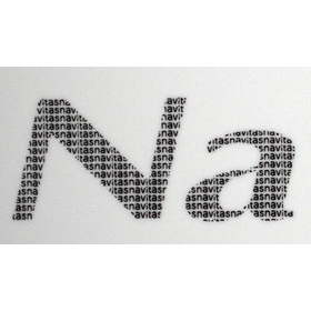
Fine printing technology for pad printing of electronic components.

Fine part number printing is also clear. Expanding the possibilities of pad printing.

In the electronic components industry, with the miniaturization and high density of products, there is a demand for part number printing in fine characters and symbols. Particularly, to ensure the identification of components and traceability, it is important that the printing is accurate and does not become distorted, even when small. Unclear printing can lead to incorrect identification of parts and issues in quality control. Our pad printing technology achieves fine line printing of 0.04mm and, with a plate-making precision of ±0.01mm, produces beautifully clear fine part number prints. 【Application Scenarios】 - Printing part numbers and lot numbers on small electronic components - Fine marking on circuit boards - Printing high-design logos and characters 【Benefits of Implementation】 - Improved component identification - Ensured traceability - Enhanced product quality and reliability

  • 2305?.jpg
  • 260626_インコ.png
  • Printing Machinery
  • パッド印刷微細印刷技術

Added to bookmarks

Bookmarks list

Bookmark has been removed

Bookmarks list

You can't add any more bookmarks

By registering as a member, you can increase the number of bookmarks you can save and organize them with labels.

Free membership registration

Fine printing technology for pad printing in the semiconductor industry.

Achieving fine markings. Challenging the limits of PAD printing.

In the semiconductor industry, fine and clear marking is required for product identification and traceability. Particularly in miniaturized semiconductor components, accurately printing information in limited space is crucial for quality control and defect analysis. Unclear marking can lead to incorrect identification or lack of information. Our pad printing technology meets the needs for fine marking with 0.04mm fine line printing and ±0.01mm plate accuracy. 【Application Scenarios】 - Identification marking on small semiconductor components - Fine logo printing on high-density mounting boards - Serial number printing for quality control 【Benefits of Implementation】 - Ability to print fine information clearly - Accurate marking in limited space - Improved product identification and traceability

  • 2305?.jpg
  • 260626_インコ.png
  • Printing Machinery
  • パッド印刷微細印刷技術

Added to bookmarks

Bookmarks list

Bookmark has been removed

Bookmarks list

You can't add any more bookmarks

By registering as a member, you can increase the number of bookmarks you can save and organize them with labels.

Free membership registration