iPROS Manufacturing
  • Search for products by classification category

    • Electronic Components and Modules
      Electronic Components and Modules
      59171items
    • Machinery Parts
      Machinery Parts
      74740items
    • Manufacturing and processing machinery
      Manufacturing and processing machinery
      99939items
    • Scientific and Physics Equipment
      Scientific and Physics Equipment
      35097items
    • Materials
      Materials
      37108items
    • Measurement and Analysis
      Measurement and Analysis
      55101items
    • Image Processing
      Image Processing
      15097items
    • Control and Electrical Equipment
      Control and Electrical Equipment
      53315items
    • Tools, consumables, and supplies
      Tools, consumables, and supplies
      64378items
    • Design and production support
      Design and production support
      12467items
    • IT/Network
      IT/Network
      43701items
    • Office
      Office
      13824items
    • Business support services
      Business support services
      33336items
    • Seminars and Skill Development
      Seminars and Skill Development
      6342items
    • Pharmaceutical and food related
      Pharmaceutical and food related
      30695items
    • others
      73831items
  • Search for companies by industry

    • Manufacturing and processing contract
      7338
    • others
      4996
    • Industrial Machinery
      4415
    • Machine elements and parts
      3282
    • Other manufacturing
      2888
    • IT/Telecommunications
      2551
    • Trading company/Wholesale
      2470
    • Industrial Electrical Equipment
      2298
    • Building materials, supplies and fixtures
      1812
    • software
      1635
    • Electronic Components and Semiconductors
      1567
    • Resin/Plastic
      1492
    • Service Industry
      1446
    • Testing, Analysis and Measurement
      1130
    • Ferrous/Non-ferrous metals
      983
    • environment
      696
    • Chemical
      629
    • Automobiles and Transportation Equipment
      562
    • Printing Industry
      508
    • Information and Communications
      455
    • Consumer Electronics
      416
    • Energy
      329
    • Rubber products
      313
    • Food Machinery
      307
    • Optical Instruments
      276
    • robot
      271
    • fiber
      250
    • Paper and pulp
      231
    • Electricity, Gas and Water Industry
      168
    • Pharmaceuticals and Biotechnology
      167
    • Warehousing and transport related industries
      145
    • Glass and clay products
      139
    • Food and Beverage
      128
    • CAD/CAM
      124
    • retail
      109
    • Educational and Research Institutions
      104
    • Medical Devices
      103
    • Ceramics
      98
    • wood
      88
    • Transportation
      82
    • Medical and Welfare
      63
    • Petroleum and coal products
      62
    • Shipbuilding and heavy machinery
      51
    • Aviation & Aerospace
      48
    • Fisheries, Agriculture and Forestry
      42
    • Public interest/special/independent administrative agency
      31
    • equipment
      31
    • self-employed
      24
    • Research and development equipment and devices
      24
    • Government
      23
    • Materials
      22
    • Mining
      17
    • Finance, securities and insurance
      13
    • cosmetics
      11
    • Individual
      10
    • Restaurants and accommodations
      9
    • Police, Fire Department, Self-Defense Forces
      7
    • Raw materials for reagents and chemicals
      3
    • Laboratory Equipment and Consumables
      3
    • Contracted research
      3
  • Special Features
  • Ranking

    • Overall Products Ranking
    • Overall Company Ranking
Search for Products
  • Search for products by classification category

  • Electronic Components and Modules
  • Machinery Parts
  • Manufacturing and processing machinery
  • Scientific and Physics Equipment
  • Materials
  • Measurement and Analysis
  • Image Processing
  • Control and Electrical Equipment
  • Tools, consumables, and supplies
  • Design and production support
  • IT/Network
  • Office
  • Business support services
  • Seminars and Skill Development
  • Pharmaceutical and food related
  • others
Search for Companies
  • Search for companies by industry

  • Manufacturing and processing contract
  • others
  • Industrial Machinery
  • Machine elements and parts
  • Other manufacturing
  • IT/Telecommunications
  • Trading company/Wholesale
  • Industrial Electrical Equipment
  • Building materials, supplies and fixtures
  • software
  • Electronic Components and Semiconductors
  • Resin/Plastic
  • Service Industry
  • Testing, Analysis and Measurement
  • Ferrous/Non-ferrous metals
  • environment
  • Chemical
  • Automobiles and Transportation Equipment
  • Printing Industry
  • Information and Communications
  • Consumer Electronics
  • Energy
  • Rubber products
  • Food Machinery
  • Optical Instruments
  • robot
  • fiber
  • Paper and pulp
  • Electricity, Gas and Water Industry
  • Pharmaceuticals and Biotechnology
  • Warehousing and transport related industries
  • Glass and clay products
  • Food and Beverage
  • CAD/CAM
  • retail
  • Educational and Research Institutions
  • Medical Devices
  • Ceramics
  • wood
  • Transportation
  • Medical and Welfare
  • Petroleum and coal products
  • Shipbuilding and heavy machinery
  • Aviation & Aerospace
  • Fisheries, Agriculture and Forestry
  • Public interest/special/independent administrative agency
  • equipment
  • self-employed
  • Research and development equipment and devices
  • Government
  • Materials
  • Mining
  • Finance, securities and insurance
  • cosmetics
  • Individual
  • Restaurants and accommodations
  • Police, Fire Department, Self-Defense Forces
  • Raw materials for reagents and chemicals
  • Laboratory Equipment and Consumables
  • Contracted research
Special Features
Ranking
  • Overall Products Ranking
  • Overall Company Ranking
  • privacy policy
  • terms of service
  • About Us
  • Careers
  • Advertising
  1. Home
  2. Chemical
  3. 奥野製薬工業 大阪・放出、東京、名古屋など
  4. A comprehensive reveal of plating chemicals and plating processes for semiconductors!
CATALOG
  • Dec 12, 2023
  • Added to bookmarks

    Bookmarks list

    Bookmark has been removed

    Bookmarks list

    You can't add any more bookmarks

    By registering as a member, you can increase the number of bookmarks you can save and organize them with labels.

    Free membership registration
Dec 12, 2023

A comprehensive reveal of plating chemicals and plating processes for semiconductors!

奥野製薬工業 奥野製薬工業 大阪・放出、東京、名古屋など
Semiconductor devices, interposers that relay between semiconductor devices and printed circuit boards, and the wiring of packages used for directly mounting semiconductor chips onto printed circuit boards utilize plating technology for purposes such as transmitting electrical signals, sharing power, and heat dissipation. Okuno Pharmaceutical Industry has newly developed surface treatment chemicals and plating processes for semiconductors to keep up with the evolution of semiconductors. ◆ UBM formation for aluminum electrodes on wafers Plating process and dedicated plating equipment TORYZA EL PROCESS, TORYZA EL SYSTEM ◆ For semiconductor wafers 
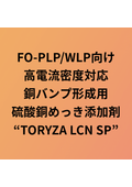
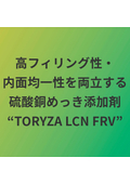
Newly developed copper sulfate plating chemicals TORYZA LCN series For more details, please contact us.
  • Inquiry about this news

    Contact Us Online
  • More Details & Registration

    Details & Registration

Related Links

Okuno Pharmaceutical Industry's homepage, introducing featured products.
For surface treatment and plating chemicals, as well as surface treatment and plating processes related to semiconductor devices, interposers, and package substrates, trust Okuno Pharmaceutical Industry.

Related product

TORYZA LCN SP製品情報.png

Copper sulfate plating additive for semiconductor wafers - TORYZA LCN SP

TORYZA LCN SP, the optimal electroplating solution for forming copper pillars on semiconductor wafers and package substrates.

Solder balls have been widely used in semiconductor packaging. However, due to the increase in pin count (the number of terminals on the substrate), the increase in the number of chips being packaged, and the reduction in bonding area, solder bumps with a diameter of about 100µm are becoming insufficient for high-density packaging. As an alternative, attention is being drawn to a method that involves forming a redistribution layer (RDL) on the semiconductor and using copper pillars for bonding. Our company has developed the optimal additive for copper pillars, TORYZA LCN SP. TORYZA LCN SP can also be used to form ultra-fine electrodes on the build-up layer of the package substrate.

  • Chemicals

Added to bookmarks

Bookmarks list

Bookmark has been removed

Bookmarks list

You can't add any more bookmarks

By registering as a member, you can increase the number of bookmarks you can save and organize them with labels.

Free membership registration
TORYZA LCN SV製品情報.jpeg

Copper sulfate plating additive for semiconductor wafers - TORYZA LCN SV

Supports high aspect ratio filling, copper sulfate plating additive for silicon interposers - TORYZA LCN SV.

With the advancement of semiconductor performance and functionality, packaging technologies related to chiplets that implement multiple chips with different functions on a single substrate and three-dimensional integration are gaining attention. Among these, silicon interposers with wiring formed on silicon are attracting interest because they can miniaturize the length and width of the wiring, thereby enhancing the transmission capability of high-frequency signals. Our company has developed TORYZA LCN SV as an additive for silicon interposers that supports high aspect ratio filling. TORYZA LCN SV excels in embedability into TSVs, achieving void-free and low film thickness high aspect ratio filling.

  • Chemicals

Added to bookmarks

Bookmarks list

Bookmark has been removed

Bookmarks list

You can't add any more bookmarks

By registering as a member, you can increase the number of bookmarks you can save and organize them with labels.

Free membership registration
TORYZA LCN SD製品情報.jpeg

Copper sulfate plating additive for semiconductor wafers - TORYZA LCN SD

Copper sulfate plating additive for semiconductor wafers, high heat dissipation and high current applications - TORYZA LCN SD.

Smartphones are widely used not only for calls but also for content viewing such as music and videos, online shopping, and in industries like automobiles, smart home appliances, and robotics. Mobile communication devices like cell phones and tablets have undergone significant evolution approximately every 10 years, with their maximum communication speeds increasing by about 1,000,000 times over the past 30 years. Additionally, semiconductors used in servers and high-performance computers are required to achieve even higher performance and multifunctionality. Our company has recently developed a new copper sulfate plating additive, TORYZA LCN SD, which is optimal for low aspect ratio via filling. TORYZA LCN SD can be widely applied to microbumps that join semiconductor chips and build-up wiring boards, as well as thermal vias used for heat dissipation in trench wiring on wafers and power semiconductors.

  • Chemicals

Added to bookmarks

Bookmarks list

Bookmark has been removed

Bookmarks list

You can't add any more bookmarks

By registering as a member, you can increase the number of bookmarks you can save and organize them with labels.

Free membership registration
TORYZA LCN FRV製品情報.jpeg

Copper sulfate plating additive for semiconductor wafers - TORYZA LCN FRV

FOWLP, FOPLP, and next-generation semiconductor package substrates, as well as ultra-fine wiring copper sulfate plating additives - TORYZA LCN FRV.

In recent years, semiconductor packaging technology has gained attention with FOWLP and FOPLP, which allow for an increase in the number of terminals relative to chip area by forming a redistribution layer on the wafer and expanding the terminals to the outside of the chip (Fan Out), in contrast to the conventional FC-BGA that is disadvantageous for thinness and cost reduction. Our company has developed a new copper sulfate plating additive for the formation of the redistribution layer in FOWLP and FOPLP. This product excels in film thickness uniformity and rectangularity of pattern shape, and it also accommodates filling of small-diameter vias. Additionally, to support the increase in the number of terminals on the chip side, the formation of ultra-fine wiring layers on the build-up layer of conventional FC-BGA is also being considered. This product is optimal for the formation of ultra-fine wiring in next-generation semiconductor package substrates.

  • Chemicals

Added to bookmarks

Bookmarks list

Bookmark has been removed

Bookmarks list

You can't add any more bookmarks

By registering as a member, you can increase the number of bookmarks you can save and organize them with labels.

Free membership registration
ubm_image.JPG

UBM formation plating process for aluminum electrodes on a wafer.

It is the process of forming UBM. It can improve the connection reliability between the aluminum electrode and the package terminal.

UBM stands for Under Bump Metal or Under Barrier Metal, and it is a film formed to join aluminum electrode pads on semiconductor chips with package terminals through wire bonding, soldering, or silver sintering. This film is composed of materials such as electroless nickel/gold plating or electroless nickel/palladium/gold plating. We offer a wide range of products that support the evolution of semiconductors and electronics, so please feel free to consult with us.

  • Chemicals

Added to bookmarks

Bookmarks list

Bookmark has been removed

Bookmarks list

You can't add any more bookmarks

By registering as a member, you can increase the number of bookmarks you can save and organize them with labels.

Free membership registration

Related catalog(5)

UBM formation plating process and dedicated equipment for aluminum electrodes on wafers.

UBM formation plating process and dedicated equipment for aluminum electrodes on wafers.

PRODUCT
  • E-book viewing
  • Catalog download

Contact this catalog

TORYZA LCN SP, a plating additive suitable for forming copper pillars on semiconductor wafers and package substrates.

TORYZA LCN SP, a plating additive suitable for forming copper pillars on semiconductor wafers and package substrates.

PRODUCT
  • E-book viewing
  • Catalog download

Contact this catalog

FOWLP, FOPLP, and copper sulfate plating additives for ultra-fine wiring such as semiconductor package substrates - TORYZA LCN FRV.

FOWLP, FOPLP, and copper sulfate plating additives for ultra-fine wiring such as semiconductor package substrates - TORYZA LCN FRV.

PRODUCT
  • E-book viewing
  • Catalog download

Contact this catalog

Copper sulfate plating additive for semiconductor wafers, high heat dissipation and high current applications - TORYZA LCN SD.

Copper sulfate plating additive for semiconductor wafers, high heat dissipation and high current applications - TORYZA LCN SD.

PRODUCT
  • E-book viewing
  • Catalog download

Contact this catalog

Copper sulfate plating additive for semiconductor wafers - TORYZA LCN SV

Copper sulfate plating additive for semiconductor wafers - TORYZA LCN SV

PRODUCT
  • E-book viewing
  • Catalog download

Contact this catalog

Distributors

奥野製薬工業
Chemical
  • Added to bookmarks

    Bookmarks list

    Bookmark has been removed

    Bookmarks list

    You can't add any more bookmarks

    By registering as a member, you can increase the number of bookmarks you can save and organize them with labels.

    Free membership registration
奥野製薬工業 大阪・放出、東京、名古屋など
  • Official site
Phone number/address

news

[Cast Iron Repair] We will repair cracks that have occurred in metal equipment without applying heat.

  • NEW
  • CATALOG

The "Mechanical Stitching Method" by Nichinichisui Road Machinery Co., Ltd. is a new technique that allows for the repair of metal cracks without the application of heat. By using special bolts and reinforcement plates, cracks are physically removed, and repairs are made without causing any thermal impact on the base material. Repairs can be carried out in environments where open flames cannot be used. Since no heat is applied, the disassembly of equipment is minimized. ◎ For more details, please contact us. ◎ If a detailed technical explanation is needed, please contact us.

May 08, 2026

Added to bookmarks

Bookmarks list

Bookmark has been removed

Bookmarks list

You can't add any more bookmarks

By registering as a member, you can increase the number of bookmarks you can save and organize them with labels.

Free membership registration

[Cast Iron Crack Repair] We repair cracks in metal products without applying heat.

  • NEW
  • COMPANY

The "Mechanical Stitching Method" by Nichinichisui Road Machinery Co., Ltd. is a new technique that allows for the repair of metal cracks without the application of heat. By using special bolts and reinforcement plates, cracks are physically removed, and repairs are made without causing any thermal impact to the base material. Repairs can be carried out in environments where open flames cannot be used. Since no heat is applied, the disassembly of equipment is minimized. ◎ For more details, please contact us. ◎ If a detailed technical explanation is needed, please contact us.

May 08, 2026

Added to bookmarks

Bookmarks list

Bookmark has been removed

Bookmarks list

You can't add any more bookmarks

By registering as a member, you can increase the number of bookmarks you can save and organize them with labels.

Free membership registration

Aluminum prototype: Lost wax casting sand mold layered 3D printer prototype.

  • NEW
  • COMPANY

● The production time for casting prototypes can be shortened! Since model production is not required, the time needed to create prototypes, which previously took about a month, can be significantly reduced. ● Model costs can be reduced! By directly producing sand molds from 3D data, there is no need for model production costs. If changes to the model are necessary, they can be addressed by modifying the 3D data. ● Similar products with different shapes and dimensions can be prototyped simultaneously! With one molding process, different products with similar shapes or varying dimensions can be molded at the same time. This allows for the verification of multiple types in a short period.

May 08, 2026

Added to bookmarks

Bookmarks list

Bookmark has been removed

Bookmarks list

You can't add any more bookmarks

By registering as a member, you can increase the number of bookmarks you can save and organize them with labels.

Free membership registration
Hotron Group Case Page

[Case Study] Hotron pursues sensor technology and creates products that generate safe and comfortable living spaces. We would like to introduce Hotron products that support people's lives throughout the city.

  • NEW
  • PRODUCT

We will introduce the implementation results of the sensor technology developed by the Hotron Group, which has been cultivated over more than half a century, through customer case studies. In addition to automatic door sensors, we also offer a wide range of vehicle detection sensors and nursing/care sensors. Many implementation examples are also presented, so please take a look at the case study page.

May 07, 2026

Added to bookmarks

Bookmarks list

Bookmark has been removed

Bookmarks list

You can't add any more bookmarks

By registering as a member, you can increase the number of bookmarks you can save and organize them with labels.

Free membership registration
Capacity Management (Medium to Large Scale)

Parking lot occupancy management vehicle detection sensor | Hotron Co., Ltd.

  • NEW
  • PRODUCT

Parking space management refers to the real-time display of parking availability and the management of efficient use of parking spaces. By utilizing Hotron's sensors, drivers can quickly discover available parking spaces, enabling efficient parking lot operations. For large parking lots, we recommend the "Floor Management Method" and "Block Management Method," which focus on cost reduction. Sensors are installed at regular intervals to count and manage the number of passing vehicles. This method offers the advantages of easy installation and low costs. 【Target Products】 - Vehicle Count Sensor CCS2 - Ultrasonic Sensor HM-UX2/UW2 For smaller facilities, we recommend the "Parking Space Management Method," where sensors are installed in each parking space to display availability with high accuracy. By providing reliable occupancy information, this method helps reduce unnecessary entry of new vehicles and ensures safe parking lot operations. 【Target Products】 - Occupancy Detection Sensor HM-UX2/UW2 - Occupancy/Pass Detection Sensor HM-LC6 - Occupancy Detection Sensor HM-LC7/LC7-FLS - Occupancy/Pass Detection Sensor HM-S6 - Occupancy Detection Sensor HM-S8

May 07, 2026

Added to bookmarks

Bookmarks list

Bookmark has been removed

Bookmarks list

You can't add any more bookmarks

By registering as a member, you can increase the number of bookmarks you can save and organize them with labels.

Free membership registration
Return to news list
  • 展示会出展等の販売促進に必要な費用を助成します! 最大300万円 助成率1/2以内 市場開拓助成事業 展示会等参加費・印刷物制作費・動画制作費 など 申請受付:令和8年 5/15(金)~5/29(金)
    • Inquiry about this news

      Contact Us Online
    • More Details & Registration

      Details & Registration

    Products

    • Search for Products

    Company

    • Search for Companies

    Special Features

    • Special Features

    Ranking

    • Overall Products Ranking
    • Overall Company Ranking

    support

    • site map
    IPROS
    • privacy policy Regarding external transmission of information
    • terms of service
    • About Us
    • Careers
    • Advertising
    COPYRIGHT © 2001-2026 IPROS CORPORATION ALL RIGHTS RESERVED.
    Please note that the English text on this page is automatically translated and may contain inaccuracies.