We will be exhibiting at the Semiconductor and Sensor Packaging Exhibition / the Specialized Exhibition for Semiconductor Backend Processes (ISP).
Okuno Pharmaceutical Industry has developed new surface treatment chemicals and plating processes for semiconductors to respond to the evolution of semiconductors.
The new products will be introduced at the 25th Semiconductor and Sensor Packaging Exhibition, which will be held at Tokyo Big Sight from January 24 (Wednesday) to January 26 (Friday), 2024.
At the venue, we will present plating chemicals and processes for semiconductor wafers and package substrates, ultra-fine wiring, and the latest surface treatments for power devices, under the theme of OKUNO contributing to the development of printed circuit boards and semiconductor package substrates.
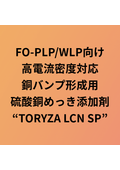
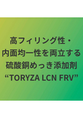
We will also showcase the new "TORYZA" series for semiconductor back-end processes, including an electroless plating process for UBM formation on wafers and dedicated plating equipment, so please stop by.
For more details, please check the related link [Exhibiting at the Semiconductor and Sensor Packaging Exhibition/Specialized Exhibition for Semiconductor Back-End Processes (ISP)].

Inquiry about this news
Contact Us OnlineMore Details & Registration
Details & Registration
Related Links
Our company will be exhibiting at the 25th Semiconductor and Sensor Packaging Exhibition, which will be held at Tokyo Big Sight from January 24 (Wednesday) to January 26 (Friday), 2024. We will showcase our new product series "TORYZA" for semiconductor backend processes, including an electroless plating process for UBM formation for wafers and dedicated plating equipment. We look forward to your visit.
Related product


Related catalog(5)