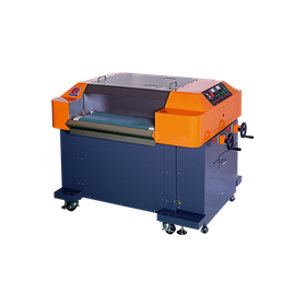
● Down-cutting method using diamond wire ● No slurry required due to fixed abrasives ● Compatible with wafer processing of small diameters up to 4 inches
- Compatible with wafer processing of small diameters up to 4 inches - Down-cut method using high-performance electroplated diamond wire - No slurry required due to fixed abrasives - Capable of processing various materials by changing wire speed - Square cutting is also possible - High-precision processing of all hard and brittle materials is possible
Inquire About This Product
basic information
【Specifications】 Work dimensions: 100×100mm Wire travel method: Reciprocating Wire speed: 1–200m/min Cutting method: Down cut Cutting feed speed: 0.01–5mm/min Rapid feed speed: 150mm/min (Max. 500m/min) Wire diameter: 0.15–0.35mm Main body size: 780(D)mm × 1310(W)mm × 1840(H)mm Weight: Approximately 600Kg Input power supply: 3-phase 3-wire AC200V 30A
Price range
Delivery Time
Applications/Examples of results
- Compatible with wafer processing of small diameters up to 4 inches - Down-cutting method using high-performance electroplated diamond wire - No slurry required due to fixed abrasives - Capable of processing various materials by changing wire speed - Square cutting is also possible - High-precision processing of all hard and brittle materials is possible
catalog(1)
Download All CatalogsCompany information
July 2009: Received certification for a research and development plan related to the advancement of manufacturing infrastructure technology for small and medium-sized enterprises from the Ministry of Economy, Trade and Industry. June 2010: Began joint development with the National Institute of Advanced Industrial Science and Technology on glass etching for solar cells. February 2011: Ordered and received an 8-inch chemical cleaning system for the 3D semiconductor research center. July 2011: Contracted by Saitama Prefecture for the next-generation industry entry support project. November 2011: Developed an alkaline spin etching system. Specifications: For large substrates (300 mm square). February 2012: Completion of the next-generation industry entry support project in Saitama Prefecture. April 2012: Newly developed silicon wafer separator for solar cells.


![Deburring Machine "Twin Baritor" [Eligible for Small and Medium Enterprise Productivity Investment Subsidy]](https://image.mono.ipros.com/public/product/image/6d3/2000308654/IPROS16685940644635288329.png?w=280&h=280)


