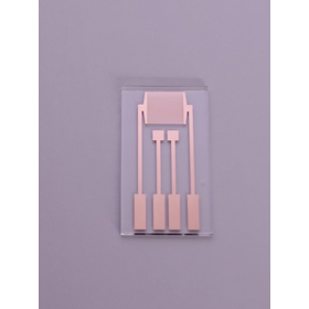
This is a "comb-shaped electrode chip" made by thin-film pattern processing of various metals. We handle everything from electrode configuration to thin-film processing and chip processing in a consistent system.
Are you troubled by such issues? - It’s difficult to manage delivery times when ordering thin film processing and pattern processing separately. - I haven’t put it into a drawing, but could you provide some consultation? - I want to achieve fine wiring, but I would like advice on the deposition materials. - Can you accept orders for pattern processing alone? - Can you accommodate a line and space (L/S) of 10μm? ■ Microfabrication Technology We realize fine patterning through photolithography, etching, and metal masks. Depending on customer requirements, we select the best processing methods and resists. However, it is necessary to align conditions such as deposition materials, substrates, film thickness, and thin film stacking configurations. Please consult us regarding sub-micron or nanometer level patterns. ■ Small-scale prototyping is also possible. In manufacturing, the cycle of hypothesis and verification is an essential process. No matter how advanced simulation technology becomes, verification cannot be omitted. Therefore, at Adachi New Industry, we are happy to undertake prototyping for characteristic verification. Please contact us first.

Inquire About This Product
basic information
1) Thin Film Deposition Achievements Using vacuum deposition and sputtering processes, we can create films with a variety of metals and dielectrics. We have a wide range of substrate types with proven results. We will propose the optimal thin film configuration. ■ Metal/Alloy Single Layer Films Au, Ag, Pt, Cu, Ti, Cr, Ni, Al, DLC, ITO, and other metals and alloys ■ Dielectric Films Various metal oxides, nitrides, insulating films, etc. ■ Compatible Substrates Various glasses, resins, films, and various wafers (Si, SiC, Ge, GaN, etc.) ■ Work Size We can accommodate sizes up to 150mm. 2) Fine Pattern Processing Accuracy Electrode line width: a few μm, electrode spacing: a few μm, film thickness: from several tens of nm to a few μm 3) Integrated Production from Substrate Procurement to Film Deposition At Adachi New Industry, we can provide a fully customized service from substrate procurement to film processing, fine processing, and chip processing. It is also possible to cut to any shape and ship as components. 4) Clean Room Compliance The working environment maintains the necessary cleanliness levels from film deposition to inspection, and we have a robust system in place to address minor film defects (such as foreign particles in the film).
Price information
It will vary depending on the quantity, size, and pattern accuracy. Please feel free to contact us first. We would appreciate it if you could provide the following information simultaneously to facilitate a smooth proposal: - Purpose - Information about the metal film: number of layers, thickness - Substrate information: glass, resin, Si wafer, SiC wafer, etc. - Product size, thickness - Pattern drawings - Final product (as much information as you can share).
Delivery Time
Applications/Examples of results
- Electrochemical analysis chip - Bioscience, organic electronics - TEG chip - Organic semiconductor analysis electrode - Electrodes for various sensors (e.g., gas sensors) - Electrode for SOFC (solid electrolyte) materials, etc.
catalog(3)
Download All Catalogs


News about this product(37)


Company information

Since our founding in Taisho 8 (1919), we have cultivated an extensive network as a chemical industrial trading company and will respond to all of our customers' needs through various surface treatment technologies, including optical thin film processing (optical coating). Company Name: Adachi Shinsangyo Co., Ltd. Representative Director: Kensuke Adachi Capital: 10 million yen Founded: November, Taisho 7 (1918) Established: August, Showa 39 (1964) Location: ■ Head Office: 10F Anix Building, 1-14-20 Tachiuri-bori, Nishi-ku, Osaka 550-0012 Phone: 06-6536-2051 / FAX: 06-6536-2015 ■ Higashi-Osaka Factory: 3-3-1 Tamakushicho Higashi, Higashi-Osaka City 578-0932 Phone: 072-962-4133 / FAX: 072-964-9055 Group Companies: Osaka Vacuum Industry Co., Ltd., Adachi Kousan Co., Ltd.

![Electrode processing [copper electrodes, graphite electrodes]](https://image.mono.ipros.com/public/product/image/373/2001534434/IPROS9289249261800395293.png?w=280&h=280)
![[Example of Prototype Press Processing] 'Custom Electrode' Copper C1100](https://image.mono.ipros.com/public/product/image/c4f/2001132679/IPROS21678739218728070024.png?w=280&h=280)


![Powerful Compact Crusher "Force Mill" [Tea Leaves, Tablets, Grains]](https://image.mono.ipros.com/public/product/image/83f/226060010/IPROS6786981127584100059.jpg?w=280&h=280)


