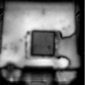
Ultrasonic microscope observation of transistors! It is possible to check the peeling conditions at various locations even with the same focus.
We would like to introduce our ultrasonic microscope observation of semiconductor packages. Due to storage conditions and mounting conditions, delamination can occur between the metal parts (die pad) and the package resin in semiconductor packages. Delamination inside the package is a defect that significantly affects product quality, but it cannot be confirmed visually from the outside. By using an ultrasonic microscope, we can clearly capture the internal structure of the package and contribute to reliability evaluation. 【Features】 ■ Ultrasonic microscope observation from the chip side - By changing the focal position, previously unseen areas of the same sample become visible. ■ Ultrasonic microscope observation from the die pad side - Delamination conditions can be confirmed at various locations even with the same focus. *For more details, please download the PDF or feel free to contact us.
Inquire About This Product
basic information
For more details, please download the PDF or feel free to contact us.
Price range
Delivery Time
Applications/Examples of results
For more details, please download the PDF or feel free to contact us.
catalog(4)
Download All Catalogs


News about this product(1)

Company information

Aites was established in 1993, originating from the quality assurance department of the IBM Japan Yasu office. Based on the technical expertise cultivated through cutting-edge defect analysis and reliability assurance of electronic components at the IBM Japan Yasu office, we have provided various products and services that support the development and manufacturing of semiconductors, displays, organic EL, solar cells, and electronic components to customers both domestically and internationally.

![[C-SAM] Ultrasonic Microscopy Method](https://image.mono.ipros.com/public/product/image/dda/2000387315/IPROS30609954037734018246.jpeg?w=280&h=280)

![[Analysis Case Study] Observation of Adhesion State Through Metal Plates Using Ultrasonic Microscopy](https://image.mono.ipros.com/public/product/image/367300/IPROS2705829217984245675.png?w=280&h=280)


