Ultrasonic microscope observation of semiconductor packages
This is an introduction to the ultrasonic microscope observation of semiconductor packages conducted by our company.
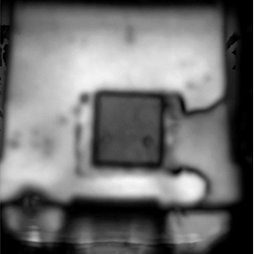
Due to storage conditions and mounting conditions, delamination may occur between the metal parts (die pad) and the package resin in semiconductor packages. Delamination inside the package is a defect that significantly affects product quality, but it cannot be detected through visual inspection.
By using an ultrasonic microscope, we can clearly capture the internal structure of the package, contributing to reliability evaluation.

Inquiry about this news
Contact Us OnlineMore Details & Registration
Details & Registration
Related Links
Related product
Related catalog(3)


Distributors