
Semiconductor Manufacturing Equipmentの製品一覧
- 分類:Semiconductor Manufacturing Equipment
4141~4185 件を表示 / 全 5157 件


Reduce the workload from handling heavy objects! Here are five case studies that solved customer challenges! We are also accepting free consultations and tests tailored to your work!

- Other conveying machines


Strong cold wind from room temperature to -13°C! Depending on the usage environment, you can choose between the combo type or the separate type!
- Cooling system

April 10, 2024 (Wednesday) to April 12, 2024 (Friday) Notice of Participation in Nagoya Manufacturing World 2024
Sanwa Shiki Ventilator Co., Ltd. will be exhibiting at the 2024 Monozukuri World (Nagoya) held at Port Messe Nagoya. We will also be showcasing our large cooling fans and cool/warm ambient products. Date: April 10, 2024 - April 12, 2024 Opening: 10:00 AM Location: Nagoya Port Messe (Exhibition Hall 1) *Our booth: 19-1 We would be grateful if you could visit us if you have the time.


Featuring the latest products from Tokyo Electron Kyushu, a leading company in semiconductor manufacturing equipment!
- Other semiconductor manufacturing equipment


Film formation completed without exposure to the atmosphere in full auto! ~Sample measurement in progress!~
- Sputtering Equipment

FC EXPO2016 Press Release
In the "Kyushu University Special Feature" of the Nikkan Kogyo Shimbun (11/30), we are promoting through an advertisement. Please check the press release summarizing the "Hydrogen Visualization System," which has been adopted for the next-generation rocket tests by ISAS/JAXA.


SiC semiconductor evaluation device using photoluminescence (PL) imaging method
- Semiconductor inspection/test equipment


It is a high-efficiency ozone removal device that can be used under vacuum conditions.
- Other semiconductor manufacturing equipment
- Other filters


PSPC standard compliant product. It uses a three-blade cutter, which ensures long-lasting blades and low running costs!
- Wafer processing/polishing equipment


A semi-automatic grinding machine for chamfering the outer peripheral edge of a wafer in a simple manner.
- Wafer processing/polishing equipment

This device measures the thickness of wafers fixed to ceramic plates without contact, using optical probes/sensors.
- Semiconductor inspection/test equipment
- Other semiconductor manufacturing equipment

This machine is a device for measuring the thickness of φ8” silicon wafers.
- Semiconductor inspection/test equipment
- Other semiconductor manufacturing equipment

This machine is a device that performs macro and micro inspections of φ8-inch wafers in the semiconductor manufacturing process.
- Semiconductor inspection/test equipment
- Other semiconductor manufacturing equipment


It is a diamond-like carbon that is resistant to wear.
- Coater

This machine is a device for spin-drying workpieces.
- Other semiconductor manufacturing equipment
- Other industrial robots

It is a device for drying wafers that have been stripped and cleaned.
- Semiconductor inspection/test equipment
- Other semiconductor manufacturing equipment

It is a device for cleaning wafers that are epoxy bonded to a glass plate.
- Other semiconductor manufacturing equipment
- Wafer processing/polishing equipment
- Other industrial robots

It is a device for applying a solution by spin coating.
- Wafer processing/polishing equipment
- Other industrial robots
- spray

It is a semi-automatic device for visual inspection of 8-inch silicon wafers.
- Semiconductor inspection/test equipment
- Other semiconductor manufacturing equipment

This is a fixture for visual inspection of the front and back surfaces of the quartz mask.
- Semiconductor inspection/test equipment
- Other semiconductor manufacturing equipment

This is a device for visual inspection and thickness measurement of 8-inch silicon wafers.
- Semiconductor inspection/test equipment
- Other semiconductor manufacturing equipment

It is a device that performs macro inspection of wafers and micro inspection using a microscope.
- Semiconductor inspection/test equipment
- Other semiconductor manufacturing equipment
This is a device for surface inspection of wafers after polishing.
- Semiconductor inspection/test equipment
- Other semiconductor manufacturing equipment

Two-dimensional code reading device
- Other semiconductor manufacturing equipment
- Other semiconductor manufacturing equipment

This is a device for visually inspecting the edges of φ300 mm silicon wafers (chip and chipping inspection).
- Semiconductor inspection/test equipment
- Other semiconductor manufacturing equipment

Pass/Fail Judgment Device
- Semiconductor inspection/test equipment
- Other semiconductor manufacturing equipment

Manual device equipped with a safety cover and remote control mechanism.
- Other semiconductor manufacturing equipment
- Other processing machines

This is a device for heating φ300mm bonded wafers using an IR lamp.
- Other semiconductor manufacturing equipment

Bulk cassette to cassette transfer
- Other semiconductor manufacturing equipment

A device capable of performing three types of operations.
- Semiconductor inspection/test equipment
- Other semiconductor manufacturing equipment

This is a device for drying 300mm wafers that have been cleaned after double-sided polishing.
- Semiconductor inspection/test equipment
- Other semiconductor manufacturing equipment

This is a device for simple cleaning (brush + water) of φ300 mm silicon wafers.
- Semiconductor inspection/test equipment
- Other semiconductor manufacturing equipment

Loading and unloading of φ150 mm and φ125 mm silicon wafers.
- Semiconductor inspection/test equipment
- Other semiconductor manufacturing equipment

This is a device for storing φ300 mm wafers, which have completed processing, one by one into a Teflon cassette for submersion.
- Semiconductor inspection/test equipment
- Other semiconductor manufacturing equipment

It is a device that loads wafers one by one.
- Semiconductor inspection/test equipment
- Other semiconductor manufacturing equipment

This is a device used for handling to perform P/N determination and visual inspection of silicon wafers.
- Semiconductor inspection/test equipment
- Other semiconductor manufacturing equipment

It is a device for inverting and transferring silicon wafers.
- Semiconductor inspection/test equipment
- Other semiconductor manufacturing equipment

Classified by resistivity and thickness categories.
- Semiconductor inspection/test equipment
- Other semiconductor manufacturing equipment

This is a device that detects the wafer edge using laser light and measures the diameter by comparing it with a calibration wafer (reference wafer).
- Semiconductor inspection/test equipment
- Other semiconductor manufacturing equipment

This is a device that detects the edge of a wafer and measures its diameter through image processing.
- Semiconductor inspection/test equipment
- Other semiconductor manufacturing equipment

This is a device that measures the thickness of sapphire wafers and sorts them according to their thickness.
- Semiconductor inspection/test equipment
- Other semiconductor manufacturing equipment

It is a device that measures the thickness of silicon wafers and rearranges them according to their thickness.
- Semiconductor inspection/test equipment
- Other semiconductor manufacturing equipment

It is a device that measures the thickness of silicon wafers and sorts them according to their thickness.
- Semiconductor inspection/test equipment
- Other semiconductor manufacturing equipment

It is a device that measures the thickness of silicon wafers and sorts them according to their thickness.
- Semiconductor inspection/test equipment
- Other semiconductor manufacturing equipment

This is a device used to measure the thickness of metal or resin carriers used in the silicon wafer lapping process and double-sided polishing process.
- Semiconductor inspection/test equipment
- Other semiconductor manufacturing equipment
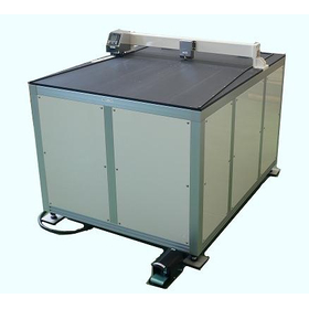
This is a device used to measure the thickness of metal or resin carriers used in the silicon wafer lapping process and the double-sided polishing process.
- Semiconductor inspection/test equipment
- Other semiconductor manufacturing equipment

This is a device used to measure the thickness of metal or resin carriers used in the silicon wafer lapping process and the double-sided polishing process.
- Semiconductor inspection/test equipment
- Other semiconductor manufacturing equipment

Thickness measurement of compound semiconductor wafers in sizes φ2”, φ4” or φ6”.
- Semiconductor inspection/test equipment
- Other semiconductor manufacturing equipment

Thickness measurement of various types of wafers below φ4"
- Semiconductor inspection/test equipment
- Other semiconductor manufacturing equipment