

Electrostatic Photoresist "Elecoat EU-XC Series"
Formation of resist by electrophoretic method
It is a negative-type photoresist solution. The resist is formed using an electrophoretic method.
- Company:シミズ
- Price:Other
1~17 item / All 17 items
Formation of resist by electrophoretic method
It is a negative-type photoresist solution. The resist is formed using an electrophoretic method.

Electrodeposition process of negative-type photoresist to achieve high-precision plating areas.
The Erecote EU-XC process is a photoresist electrophoretic process that achieves high-precision partial plating on uneven surfaces and three-dimensional shapes. This electrophoretic resist has excellent chemical resistance and can be used as a resist for silver cyanide plating, as well as for gold plating and copper sulfate plating. It features excellent edge coverage and achieves high-precision developability. It is a negative-type electrophoretic photoresist that enables precise partial plating and can also be used as an etching resist.
![[Developed Product] Negative Type Anionic Electrophoretic Photoresist](https://image.mono.ipros.com/public/product/image/7c6/2001425387/IPROS60122774361252602580.png?w=280&h=280)
It is a negative-type anion electrostatic photoresist!
Since it is an anionic electrophoretic negative-type photoresist, the developer and stripping solution will be alkaline. The developer and stripping solution are not specialized products.

An explanation of the basic knowledge of photoresist, which is essential for semiconductor manufacturing.
In the semiconductor manufacturing industry, a precise understanding and application of photoresist is essential for the formation of fine circuits. Particularly, the accuracy of circuit patterns is directly linked to the performance of semiconductor devices, making it important to grasp the characteristics and types of photoresist, as well as their roles in the process. Improper selection or use of photoresist can lead to reduced yield and quality issues with products. This page covers everything from the basic concepts of photoresist to the differences between negative and positive types, process images, coating methods, and the features of our electrodeposition resist, addressing any questions related to photoresist. 【Usage Scenarios】 - Circuit patterning in semiconductor manufacturing processes - Acquisition of basic knowledge about photoresist - Consideration of introducing electrodeposition resist 【Benefits of Introduction】 - Deepening understanding of photoresist - Support for appropriate photoresist selection - Streamlining manufacturing processes and improving quality

Basic knowledge of photoresists useful for manufacturing small actuators.
In the field of robotics, particularly in the manufacturing of small actuators, precise circuit formation is required. The technology for accurately transferring fine patterns directly impacts the performance and reliability of actuators. Inappropriate selection or use of photoresist can lead to circuit defects and a decrease in product lifespan. Our collection of basic knowledge on photoresist supports optimal material selection and process design by deepening understanding from the fundamentals of photoresist in response to these challenges. 【Application Scenarios】 - Precise circuit pattern formation for small actuators - Micromachining in semiconductor manufacturing processes - Material evaluation during the research and development phase 【Benefits of Implementation】 - Improved accuracy in circuit formation - Maintenance of product reliability and performance - Increased efficiency in the development process

An explanation of the basic knowledge of photoresist, which is essential for semiconductor manufacturing.
In the LED industry and the formation of light-emitting elements, the creation of fine circuit patterns significantly affects product performance. In particular, the element formation process related to light efficiency and response speed requires precise patterning technology. Inappropriate selection or use of photoresists can lead to reduced yield and failure to achieve the expected performance. This page covers the basics of photoresists, their types, process images, coating methods, and the features of our electrocoated resists, providing information that can help solve technical challenges in LED manufacturing. 【Usage Scenarios】 - Circuit patterning in LED chip manufacturing - Formation of fine light-emitting areas - Processes requiring high-precision pattern transfer 【Benefits of Implementation】 - Acquisition of basic knowledge about photoresists - Promotion of understanding of the LED manufacturing process - Provision of decision-making materials for appropriate photoresist selection

Explaining the basic knowledge of photoresist essential for microstructure processing.
In the micro-machining industry and fine structure processing, high-precision pattern formation is required. In particular, understanding the characteristics of photoresists and their appropriate selection is crucial for precisely creating fine circuits and structures. The use of inappropriate photoresists or errors in the process can lead to a decrease in the accuracy of fine structures and a deterioration in yield. This page covers everything from the basic knowledge of photoresists, their types, process images, coating methods, to the features of our electrodeposition resist, providing information that will help solve technical challenges in micro-machining manufacturing. 【Application Scenarios】 - Design of fine structures for micro-machines - Precision circuit patterning - Semiconductor manufacturing processes - MEMS device manufacturing 【Benefits of Implementation】 - Improvement in the accuracy of fine structure processing - Enhancement of yield - Promotion of understanding of manufacturing processes - Support for appropriate photoresist selection
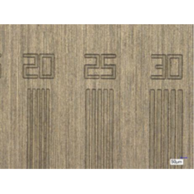
Negative-type anionic electrodeposition photoresist contributing to fine structure formation.
In the micro-machining manufacturing industry and fine structure formation, precise patterning is required. In particular, accurately reproducing complex shapes and fine irregularities is essential, as it directly affects the performance and functionality of the products, making advanced technology indispensable. Insufficient patterning can lead to reduced yield and performance issues in products. This product addresses these challenges as a negative-type photoresist for anionic electrodeposition. 【Application Scenarios】 - Precise pattern formation in micro-machining processes - Manufacturing of components with fine structures - Fields requiring high-precision surface processing 【Benefits of Implementation】 - Supports accurate formation of fine structures - Potentially contributes to improved product performance - May enhance the efficiency of development and manufacturing processes
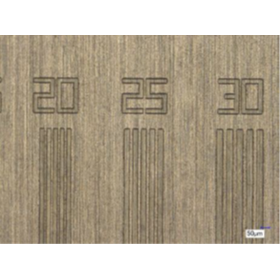
Negative-type anionic electrophoretic photoresist contributing to pixel electrode formation.
In the display manufacturing industry, particularly in pixel electrode formation, fine and uniform patterning is required. High resolution and reproducibility are directly linked to the quality of the display, making the performance of photoresists extremely important. Improper development or stripping can lead to defects and potentially affect product yield. This product addresses these challenges as an anionic electrophoretic negative-type photoresist. 【Application Scenarios】 - Formation of pixel electrodes for display panels - Manufacturing of electronic components requiring fine patterning 【Effects of Implementation】 - Improved patterning accuracy through uniform development and stripping - Applicability to uses that leverage the characteristics of the developed product
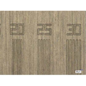
For the formation of wiring patterns in printed circuit board manufacturing. Negative-type anionic electrodeposition photoresist.
In the formation of wiring patterns for printed circuit board manufacturing, the creation of fine and precise circuit patterns is required. Particularly, to consistently produce reliable products, the uniform application of photoresist and the certainty of the development and stripping processes are crucial. Inadequate pattern formation can lead to circuit disconnections or shorts, potentially causing a decline in product quality and defects. This product contributes to solving the challenges of wiring pattern formation in printed circuit board manufacturing as a negative-type photoresist for anionic electrodeposition. 【Usage Scenarios】 - Formation of wiring patterns for printed circuit boards - Patterning of fine circuits 【Effects of Implementation】 - Formation of accurate circuit patterns - Improvement in product reliability
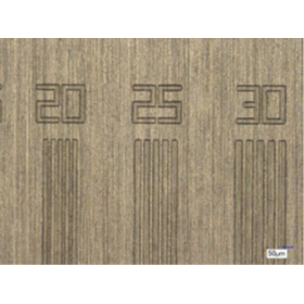
Negative-type anion electrodeposition photoresist contributing to the formation of solar cell electrodes.
In the energy sector, particularly in the formation of solar cell electrodes, precise patterning and high reliability are required. High-precision photoresist technology is essential for achieving miniaturization of electrodes and complex structures. Inappropriate resist materials or processes can lead to a decline in electrode performance and an increase in manufacturing costs. Our negative-type anionic electrodeposition photoresist has been developed to address these challenges. 【Application Scenarios】 - Patterning in the formation of solar cell electrodes - Other fields of electronic components requiring precise pattern formation 【Benefits of Implementation】 - High-precision pattern formation in solar cell electrode formation - A product in the development stage, with the potential for adjustments to meet customer needs

Fundamental knowledge of photoresist essential for microstructure processing in MEMS.
In the field of MEMS, high-precision pattern formation is required for microstructure processing. Particularly, understanding the properties of photoresists and selecting the appropriate ones are crucial for accurately creating fine circuits and structures. The use of inappropriate photoresists or errors in the process can potentially affect the reproducibility of microstructures and the performance of devices. This page explains the basic knowledge of photoresists, their types, process images, coating methods, and the features of our electrostatic resist, contributing to solving challenges in microstructure processing in the MEMS field. 【Application Scenarios】 - Prototyping and development of MEMS devices - Formation of fine circuit patterns - Product development requiring high-precision structural processing 【Benefits of Introduction】 - Acquisition of basic knowledge about photoresists - Promotion of understanding of negative and positive types - Visualization of process images - Understanding of the coating methods for liquid photoresists - Grasping the characteristics of electrostatic resist

Explaining the basic knowledge of photoresist essential for high-density packaging.
In the microelectronics industry, particularly in high-density packaging, there is a demand for technologies that can accurately form fine circuit patterns. Photoresist plays a very important role in this microfabrication process as a photosensitive material that enables pattern formation through exposure. Inappropriate selection or use of photoresist can lead to a decrease in circuit accuracy and the occurrence of defects. Our company has been responding to our customers' advanced needs through the manufacturing and sales of electrodeposited resist. In light of the importance of providing information on the basic knowledge of photoresist, we have created this basic knowledge page. It explains the fundamental mechanisms of photoresist, the differences between negative and positive types, specific process images, and the application methods for liquid photoresist. Additionally, we also introduce the features of our electrodeposited resist, so please feel free to download the catalog. 【Usage Scenarios】 - Fine circuit patterning in semiconductor manufacturing - Manufacturing processes for high-density packaging substrates - Precision processing of electronic components 【Benefits of Implementation】 - Improved accuracy of circuit patterns - Stabilization of manufacturing processes - Enhanced product reliability

Basic knowledge of photoresists useful for microchannel formation.
In the field of biochips and the formation of microfluidic channels, precise patterning is required. Particularly, the appropriate selection and application of photosensitive materials are crucial for accurately creating fine structures. Inappropriate materials or processes can lead to variations in channel dimensions and functional failures. This page explains the fundamental knowledge of photoresists, which are essential for semiconductor manufacturing, and provides information that can help solve your challenges. 【Use Cases】 - Formation of microfluidic channels in biochips - Situations requiring precise patterning 【Benefits of Implementation】 - Supports the precise formation of microfluidic channels - Contributes to improved product reliability

Explaining the basic knowledge of pattern formation for the light-emitting layer in LED manufacturing.
In the LED manufacturing industry, high-precision formation of light-emitting layer patterns is required. Particularly when forming fine circuits, understanding the characteristics of photoresist and its proper use can significantly impact product performance and yield. Without basic knowledge of photoresist, achieving the desired pattern formation may become difficult. This page covers everything from the basics of photoresist to its types, process images, coating methods, and the features of our electrocoated resist, providing information to deepen the understanding of light-emitting layer pattern formation in LED manufacturing. 【Application Scenarios】 - Formation of LED light-emitting layer patterns - Formation of fine circuits - Semiconductor manufacturing processes 【Benefits of Introduction】 - Acquisition of fundamental knowledge about photoresist - Improved understanding of the pattern formation process - Stabilization of product quality
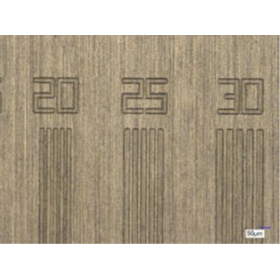
Negative-type anionic electroplating photoresist supporting fine circuit formation.
In the formation of fine circuits for semiconductor manufacturing, high-precision patterning is required. Particularly in complex circuit designs, uniform application of photoresist and accurate exposure and development processes are essential for the performance and reliability of the products. Improper pattern formation can lead to circuit shorts, disconnections, and performance degradation. This product, as a negative-type photoresist for anionic electrodeposition, uses alkaline solutions for the developer and stripping solution, and supports development in sodium carbonate aqueous solution and stripping in sodium hydroxide. [Application Scenarios] - Fine circuit patterning on semiconductor wafers - Precise resist application in electronic component manufacturing [Effects of Implementation] - Achieving high-precision fine circuit formation - Contributing to improved yield - Supporting the manufacturing of reliable semiconductor products
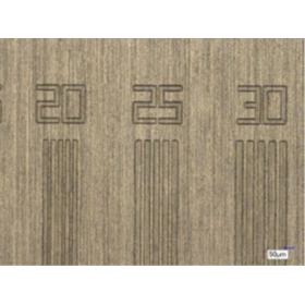
Negative-type anionic electrodeposition photoresist ideal for sensor coating.
In the automotive parts manufacturing industry, particularly in sensor coating, precise pattern formation and high reliability are required. To maximize the performance of sensors and maintain stable operation even in harsh usage environments, a photoresist capable of accurately forming fine circuit patterns is essential. Our negative-type anionic electrodeposition photoresist is compatible with the anionic electrodeposition process and can be processed with alkaline developing and stripping solutions. This enables precise coating on sensor surfaces and contributes to the improvement of product quality. 【Application Scenarios】 - Circuit pattern formation for automotive sensors - Application to electronic components requiring precise coating 【Benefits of Implementation】 - Improved sensor performance through high-definition pattern formation - Extended product lifespan due to reliable coating - Compatibility with alkaline developing and stripping solutions
