
![[Analysis Case] Evaluation of Film-Forming Component Encroachment on the Back Surface of the Wafer](https://image.mono.ipros.com/public/product/image/7cd/2000244288/IPROS4584994340989128982.jpg?w=280&h=280)
[Analysis Case] Evaluation of Film-Forming Component Encroachment on the Back Surface of the Wafer
Quantitative evaluation of metal components is possible near the bevel area.
In semiconductor device manufacturing, it is necessary to remove metals remaining on the backside of the wafer from the perspective of improving yield, and it is important to quantitatively understand the amount of metal components remaining. To investigate the concentration distribution of metals remaining on the backside within a range of 500 µm from the bevel area, we conducted evaluations using TOF-SIMS. TOF-SIMS has the spatial resolution to detect metal components only near the bevel area, and by using standard samples with known concentrations, it is possible to quantitatively calculate the concentrations.
- Company:一般財団法人材料科学技術振興財団 MST
- Price:Other
![[Analysis Case] Evaluation of Layer Structure and Film Thickness of Naturally Oxidized Copper (Cu) Surface Film](https://image.mono.ipros.com/public/product/image/321/2000246635/IPROS13899729595871211119.png?w=280&h=280)
![[Analysis Case] Evaluation of Organic EL Devices Using MSDM](https://image.mono.ipros.com/public/product/image/8f6/2000247149/IPROS1034869579092862286.jpg?w=280&h=280)
![[Analysis Case] Analysis of Discoloration Components in Fibers](https://image.mono.ipros.com/public/product/image/514/2000268026/IPROS2745253716703276512.jpg?w=280&h=280)
![[Analysis Case] Qualitative and Imaging Analysis of Micro Areas Using TOF-SIMS](https://image.mono.ipros.com/public/product/image/dbd/2000287063/IPROS7457515137597281490.jpg?w=280&h=280)
![[Analysis Case] Evaluation of Transdermal Absorption of Indomethacin in Three-Dimensional Cultured Human Skin](https://image.mono.ipros.com/public/product/image/98a/2000309800/IPROS7545183631198236681.jpg?w=280&h=280)
![[Analysis Case] Evaluation of Material Structure of Organic EL (OLED)](https://image.mono.ipros.com/public/product/image/74a/2000332445/IPROS6719634173671350524.jpg?w=280&h=280)
![[Analysis Case] Transdermal Absorption Evaluation Using Three-Dimensional Cultured Human Skin](https://image.mono.ipros.com/public/product/image/87d/2000343155/IPROS74140048043276338144.jpeg?w=280&h=280)
![[Analysis Case] LC/MS/MS Analysis of Catechin Metabolites in Urine](https://image.mono.ipros.com/public/product/image/b50/2000354279/IPROS2193284344149957247.jpg?w=280&h=280)


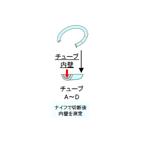
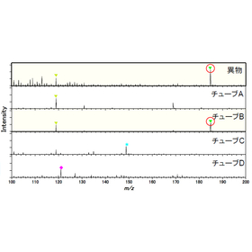
![[Analysis Case] Investigation of Foreign Object Occurrence: Analysis of the Tube](https://image.mono.ipros.com/public/product/image/387108/IPROS13070285683371051248.jpg?w=280&h=280)
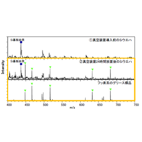
![[Analysis Case] Contamination Analysis in Vacuum Equipment](https://image.mono.ipros.com/public/product/image/387108/IPROS13932670314706549653.jpg?w=280&h=280)
![[Information] Rapid Identification of Microorganisms Using MALDI-TOF MS](https://image.mono.ipros.com/public/product/image/03c/2000704160/IPROS72307498021904210492.png?w=280&h=280)


![[Application Data] Example of Analysis of Cationic Surfactants](https://image.mono.ipros.com/public/product/image/419/2000813362/IPROS90828576391637526818.png?w=280&h=280)


![[Market Report] Global Market for Analytical Instruments](https://image.mono.ipros.com/public/product/image/391/2000957389/IPROS64018427302850551031.jpeg?w=280&h=280)
