[Measurement Example] Non-contact measurement of wafer thickness from above and below | Spectral Confocal Displacement Sensor SCI04025
SinceVision SinceVision
Detecting minute thickness changes in wafers non-contactly.
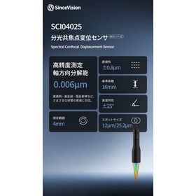
We present a case study of thickness measurement of semiconductor wafers using SinceVision's spectral confocal displacement sensor "SCI04025."
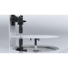
■ Thickness measurement with two sensors positioned above and below
Sensors are arranged facing each other on the top and bottom sides of the wafer, and thickness is calculated from the measurement data of both sides. Thickness can be confirmed without touching the measurement target.
■ Evaluating measurements during movement
Two points on the wafer were targeted, and automatic measurement was simulated by moving the stage. The changes in thickness and the repeatability of measurements were confirmed under dynamic conditions.
■ Maximum fluctuation of 0.6μm in 10 dynamic measurements
In this case study, the difference between the maximum and minimum thickness measurement values was up to 0.6μm. We present the evaluation results aimed at wafer thickness management.
*The values are based on the evaluation conditions of this case study and do not represent the resolution or measurement accuracy of the sensor alone. For more details, please refer to the related links or contact us.
Inquiry about this news
Contact Us Online
Distributors