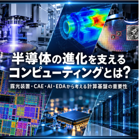
[Technical Column Release] What is the computing that supports the evolution of semiconductors? An explanation of the importance of CAE, AI, EDA, and HPC infrastructure!
 アプライド
As semiconductor miniaturization and high integration progress, the importance of high-performance computing environments that support design, manufacturing, and inspection is increasingly rising.
This time, Applied has published a technical column explaining the role of computing technology in the semiconductor industry and how to choose the optimal HPC and workstation environments.
In this article, we introduce specific application areas, including optical, structural, thermal, and fluid simulations essential for the development of semiconductor exposure equipment, design verification through CAE, detection of fine defects using AI, and circuit design and verification through EDA.
Furthermore, we explain the key points for selecting computing environments tailored to applications, such as CPU and GPU performance, memory capacity, storage, and software compatibility.
This content is highly recommended for engineers and R&D personnel at semiconductor manufacturers, manufacturing equipment manufacturers, and research institutions who are considering accelerating analysis, implementing AI, or updating computing environments.
We encourage you to take this opportunity to check it out.
Inquiry about this news
Contact Us OnlineMore Details & Registration
Details & Registration
Related Links
Related product

Related catalog(7)




Distributors