

It is a system that enables simple and rapid detection of Raman scattering.
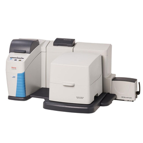
The "MultiSpec(R) Raman Spectrometer" is a system that integrates a laser light source and a spectrometer module into a dedicated 19-inch rack, enabling quick and easy detection of Raman scattering. It is designed not only for research purposes but also for use in field process lines. The built-in spectrometer utilizes a high-sensitivity spectrometer from Carl Zeiss, ensuring long-term stability. The spectroscopic section has no moving parts, eliminating the need for maintenance. 【Features】 ○ Semiconductor laser with temperature control function → Laser wavelength is 785nm, with an output of 50-50mW for excitation ○ Spectrometer resolution is 5cm⁻¹ ○ Dedicated Raman probes are custom-made with focal lengths of the front window tailored to the sample ○ Software customization is available For more details, please contact us or download the catalog.

Inquire About This Product
basic information
【Specifications】 [Laser Unit] ○ Laser Type: Fiber-coupled, stabilized power supply multi-mode semiconductor laser ○ Wavelength: 785nm ○ Output: 50-500mW, adjustable ○ Output Port: FC-APC, core diameter 105um ○ Laser Class: 3B ○ Interlock: 4 locations (key switch, probe connection, 2 external locations) [Spectrometer Unit] ○ Spectrometer Type: Carl Zeiss, MCS-CCD UV-NIR ○ Detector Used: Hamamatsu Photonics, Peltier-cooled backside illumination 2D CCD ○ Target Wavelength Range: 300-3100cm⁻¹ ○ Resolution: 3ms–10ms ○ Exposure Time: 5cm⁻¹ typ. [Fiber Probe Unit] ○ Focal Plane: From the window section at 1.5, 7.5, and parallel light ○ Fiber Length: 2m standard. Other lengths available [Others] ○ Power Supply: 110/220V; 50/60Hz ○ Dimensions: 132.55 x 448.9 x 375.5 mm³ ○ Weight: 12 – 15kg ○ Operating Temperature: 5°C – 35°C ● For more details, please contact us or download the catalog.
Price information
Please contact us.
Delivery Time
※Please contact us.
Applications/Examples of results
For more details, please contact us or download the catalog.
Company information

Mainly utilizing optical measurement, devices for various non-destructive, non-contact measurements and semiconductor manufacturing process inspections (such as film thickness measurement and plasma monitoring) are developed for both online and offline use.




![[Raman Spectrometer Technical Document] Confirmation Test of Commercial Cold Medicine Brands Based on p-Values](https://image.mono.ipros.com/public/product/image/418/2000401714/IPROS95431826680918190735.jpeg?w=280&h=280)
![Near-infrared analyzer: Comparison of dispersed and Fourier transform technologies [Technical Document]](https://image.mono.ipros.com/public/product/image/fb2/2000408775/IPROS15544504040263698443.jpeg?w=280&h=280)