Leave the implementation challenges to us! We will propose solutions with our unique design and know-how.
We propose unique design and implementation know-how using the technology accumulated through various achievements, covering package structure, bonding methods, and material selection. With our technical expertise and know-how in bonding methods for semiconductor bare chips, measurement, inspection, and reliability evaluation, we support our customers in solving their challenges. 【Challenges → Solutions】 ■ Want to implement without voids → Design and create dedicated FC fixtures ■ Want to use FC but can only obtain chips individually → Form bumps on individual pieces using a bump bonder ■ Implementing at an overseas factory but yield is not improving → Reassess conditions within our company. Reproduce NG and point out areas for review. *For more details, please refer to the PDF document or feel free to contact us.

Inquire About This Product
basic information
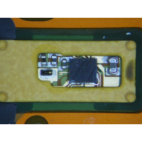
【Implementation Targets】 ■ Wire Bonding ■ Flip Chip ■ Bump Processing ■ Shear and Pull Measurement ■ Cross-Section Polishing ■ X-Ray Inspection ■ SAT *For more details, please refer to the PDF document or feel free to contact us.
Price range
Delivery Time
Applications/Examples of results
For more details, please refer to the PDF document or feel free to contact us.
catalog(1)
Download All Catalogs![[Case Study] COB High-Density Packaging](https://image.mono.ipros.com/public/catalog/image/01/508/405549/IPROS42415345949277545615.jpeg?w=120&h=170)
Company information

This is a company that handles contract manufacturing and sales of image monitoring systems, electronic devices, and system in package located in Okaya City, Nagano Prefecture.

![[Data] High-Density Mounting Specifications](https://image.mono.ipros.com/public/product/image/38c/2001502085/IPROS94455428813819361877.png?w=280&h=280)
![High-Density Implementation Products [Contract Design and Manufacturing Examples]](https://image.mono.ipros.com/public/product/image/9ae/2001288801/IPROS55317768267718714053.jpeg?w=280&h=280)


![[Case Studies] Coolant Tank Unit - 7 Examples of Production](https://image.mono.ipros.com/public/product/image/f71/2001010763/IPROS55724470191351728853.jpeg?w=280&h=280)


