Film formation processing contract service
Sartec's film deposition technology
Proposal for "film formation processing" that supports development in the AI era. Leave everything from material selection to mass production to us.
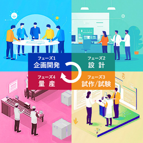
Sartec provides comprehensive support in the field of "thin film processing," which underpins the functionality of electronic products, from the design of film specifications and optimization of process conditions to mass production management. Researchers and developers involved in product development, do you have any concerns such as: "I don't know which film materials to use to meet the required functions." "I want to consider special combinations like film deposition on flexible substrates." "I want to evaluate small lot prototypes, but I don't know where to turn to." At Sartec, we propose optimal film compositions, material selections, and deposition methods to help bring your product's objectives and completion image closer to reality, and we support the establishment of a stable mass production system. Leveraging the expertise in fine structure design, material knowledge, and mass production know-how cultivated in flexible substrate design, we will work alongside you from the initial concept stage to promote manufacturing together.

Inquire About This Product
basic information
We will propose the optimal method according to your requests. 1. Target base materials (substrates) Various films Various resin sheets Various wafers Various glasses Ceramics Various metals 2. Types of films Metals (Cu, Al, Cr, Ni, Sn, Ti, Ta, W, Zn, Ag, Au, Pd, Pt, etc.) Oxide films (ITO, Al2O3, SiO2, SiO, TiO2, MgO, etc.) Nitride films (AlN, BN, SiN, TiN, etc.) Carbide films (SiC, TiC, etc.) Organic compounds (PI, PA, PE, etc.) 3. Film formation methods Sputtering method Vapor deposition method CVD method (Plasma CVD (PE-CVD), LP-CVD) Coating method (dip coat, spin coat, spray coat) Plating method (electroless plating, electroplating)
Price information
Sartec's film deposition processing specializes not only in standalone contract services but also in providing integrated solutions that combine the design of FPCs (flexible printed circuits) and electronic component mounting. We offer proposals from the perspective of "product development aimed at completion" for customers facing challenges such as "the film deposition was successful, but there were issues in the next process" or "I can't find a partner to transition from the prototype stage to mass production." #FilmDeposition, #Sputtering, #Evaporation, #CVD, #Plasma, #Coating, #ElectrolessPlating, #RollToRoll, #Wafer, #Glass
Delivery Time
Applications/Examples of results
■Regarding R to R Support With R to R (Roll-to-Roll) support, continuous and highly efficient film deposition processing is achieved for film-like materials. This enables a smooth transition from prototyping to mass production processes, balancing development speed and cost performance. For details regarding the target base materials, types of film deposition, methods of deposition, etc., please contact us. #Film Deposition, #Sputtering, #Evaporation, #CVD, #Plasma, #Coating, #Plating, #Electroless Plating, #Electroplating, #Roll-to-Roll, #Wafer, #Glass, #Ceramics #Cu, #Al, #Cr, #Ni, #Sn, #Ti, #Ta, #W, #Zn, #Ag, #Au, #Pd, #Pt, #ITO, #Al2O3, #SiO2, #SiO, #TiO2, #MgO, #AlN, #BN, #SiN, #TiN, #SiC, #TiC, #PI, #PA, #PE #Film Deposition, #Sputtering, #Evaporation, #CVD, #Plasma, #Coating, #Electroless Plating, #Roll-to-Roll, #Wafer, #Glass, #Ceramics
Company information
Sartec is a manufacturing support company based in Hamamatsu City, Shizuoka Prefecture, focused on flexible circuit board design. Going beyond our core strength and origin in "flexible circuit board design," we provide support tailored to each stage of development, from initial development to mass production, including software/hardware development, enclosure design, prototype evaluation, and manufacturing support. Printed circuit boards are an essential component often referred to as the "heart" of a product. Because we have a deep understanding of this core part, we can create a development process with minimal setbacks through our approach of "manufacturing that considers the user's experience" combined with "process design capabilities that encompass the entire product," turning the ideals of researchers and developers into tangible reality. At Sartec, we have a wide range of achievements across various fields, from cutting-edge special designs in medical and aerospace sectors to everyday products like automobiles and IoT appliances. We are also flexibly responding to the semiconductor field, which has been gaining attention in recent years, expanding the possibilities of technology through processes like film formation. If you have a desire to challenge conventional industry norms and pursue products or new technologies that do not yet exist in the world, please feel free to consult with Sartec.


