
List of Semiconductors and ICs products
- classification:Semiconductors and ICs
3796~3810 item / All 4860 items


Reduce the workload from handling heavy objects! Here are five case studies that solved customer challenges! We are also accepting free consultations and tests tailored to your work!

- Other conveying machines


No more need to lift heavy one-gallon cans! Enjoy comfortable liquid transfer in the central kitchen.
- Other Pumps
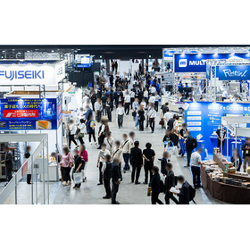
Decision to exhibit at the 1st Chubu Food Industry Creation Exhibition '26!
We will be exhibiting at the "1st Chubu Food Industry Creation Exhibition '26" to be held at Port Messe Nagoya from November 4 (Wednesday) to November 6 (Friday), 2026. As a new addition to our lineup, we will showcase the "Cordless Sanitary Handy Pump," which is a product we started selling in April last year, alongside our "Compact Sanitary Handy Pump Model MHS." - Cordless! Portable anywhere! Easy to use! Simple cleaning! It is compatible with standard 18L cans and BIB (Bag-in-Box) and features a structure that allows for easy disassembly and cleaning. We would like to invite you to visit us at this opportunity. - Venue: Port Messe Nagoya - Our exhibition booth: Hall 1 "C-66"


Developing various fine joining devices with [DDL + beam shape variable mechanism]!
- Laser Components
- Other semiconductors


We will combine our technical expertise and leverage our team strength to provide outputs that satisfy our customers.
- ASIC
- Circuit board design and manufacturing
- EMS


We will propose and manufacture test wafers for film formation processes tailored to the circumstances of each company.
- Other semiconductors
- Wafer

We will propose and manufacture test wafers for film formation processes tailored to the circumstances of each company!
At Advanced Materials Technology, we supply wafers that incorporate cutting-edge technologies necessary for research and development in film formation, CMP, cleaning, etching, and TSV, particularly for test wafers. 【Available Film Types】 Cu, Ta, TaN, Ti, TiN, Al-Cu, SiN, PE-TEOS, HDP, HARP oxide, Poly-Si, Th-Ox, ACL, SiC, SiON, Photo resist, Polyimide ■Metal-based Ru, Co, CoEP, Pt, Au, W

We will propose and manufacture test wafers for film formation processes tailored to the circumstances of each company.
- Other semiconductors
- Wafer
We will propose and manufacture test wafers for film formation processes tailored to the circumstances of each company!
At Advanced Materials Technology, we supply wafers that incorporate cutting-edge technologies necessary for research and development in film formation, CMP, cleaning, etching, and TSV, particularly for test wafers. 【Available Film Types】 Cu, Ta, TaN, Ti, TiN, Al-Cu, SiN, PE-TEOS, HDP, HARP oxide, Poly-Si, Th-Ox, ACL, SiC, SiON, Photo resist, Polyimide ■Metal-based Ru, Co, CoEP, Pt, Au, W

Very useful for CMP research and development applications! Please consult us regarding the types of membranes available according to your needs.
- Other semiconductors
- Wafer

Recommended for research purposes! Patterned wafer with HDP as the top layer.
- Other semiconductors
- Wafer

A patterned wafer close to device grade manufactured through domestic mass production.
- Other semiconductors
- Wafer

Compatible with 300mm wafers! Successfully created patterns at widths close to the target sizes of recent devices.
- Other semiconductors
- Wafer

Very useful for CMP research and development applications! Patterns with high step heights are also available.
- Other semiconductors
- Wafer

Very useful for CMP research and development! 【Pattern Wafer】 3D ILD Pattern
At Advanced Materials Technology, we supply wafers that incorporate cutting-edge technologies necessary for research and development in film formation, CMP, cleaning, etching, and TSV, particularly among test wafers. The image shows examples of HDP and SiN on Si. We can accommodate 200mm and 300mm sizes. Please consult us regarding the types of films you require. We also offer patterns with high step heights, which are very useful for CMP research and development purposes. *For more details, please download the catalog or contact us. Basic Information [About Our Services] Our company aims for rapid supply, stable supply, and more cost-effective supply of products, providing and selling wafers tailored to various customer requests. - Sales of various evaluation pattern wafers and film formation wafers - Collection and recycling of used silicon wafers - Contract analysis and evaluation services We have excellent procurement sources in the United States, Europe, South Korea, and Taiwan, and we are prepared to provide our customers with wafers of better quality in a stable manner.

Available in 200mm and 300mm! Please consult us regarding the types of films available according to your preferences.
- Other semiconductors
- Wafer

Available in 200mm and 300mm! 【Test wafer for CMP】 MIT STI CMP wafer
At Advanced Materials Technology, we supply wafers that incorporate cutting-edge technologies necessary for research and development in film formation, CMP, cleaning, etching, and TSV, particularly for test wafers. The image shows an example of HDP and SiN on Si. We can accommodate 200mm and 300mm sizes. *MIT mask used Please consult us regarding the types of films according to your preferences.

A pattern wafer manufactured in domestic mass production, close to device grade.
- Other semiconductors
- Wafer