
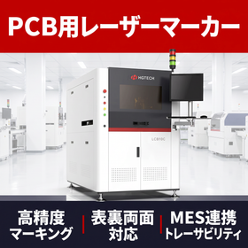
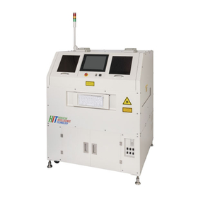
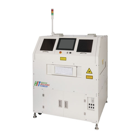
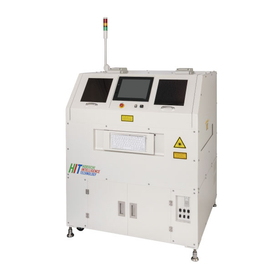
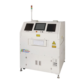
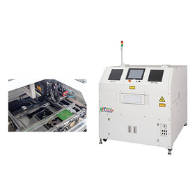
PCB Inline Laser Marker for Semiconductors
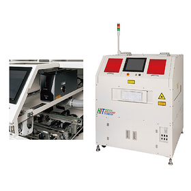
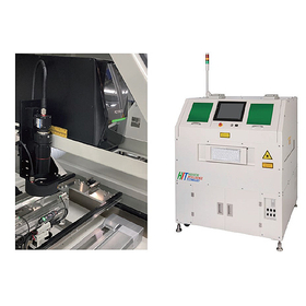
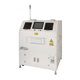
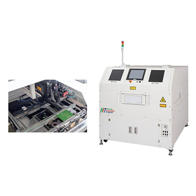
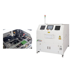
Simultaneous dual-side marking for reduced takt time. High-precision laser marking system compatible with MES integration.
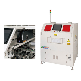
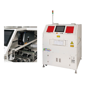
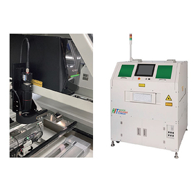
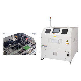
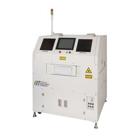
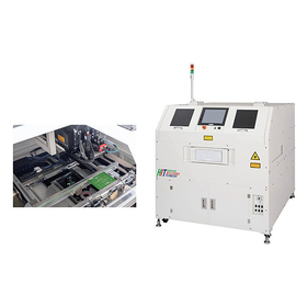
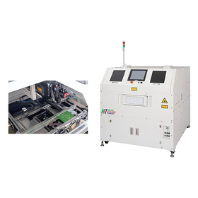
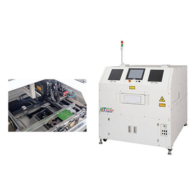
In the semiconductor industry, precise marking on substrates is essential for fine processing. Especially as products become smaller and more densely packed, ensuring the accuracy of marking and traceability is crucial for quality control and yield improvement. Misalignment and marking defects not only undermine product reliability but also lead to increased manufacturing costs. Our PCB inline laser marker achieves high-precision marking while correcting substrate misalignment through an XY drive head and CCD substrate recognition. It also enables traceability management through MES integration, contributing to quality control and efficiency in semiconductor manufacturing. 【Usage Scenarios】 - Marking of model numbers, serial numbers, logos, etc., on semiconductor substrates - High-speed marking on inline production lines - Management of manufacturing history through MES integration 【Benefits of Implementation】 - Quality improvement through high-precision marking - Reduction of tact time with dual heads - Strengthening of traceability through MES integration - Prevention of substrate contamination with dust suction mechanisms
- Company:JFE商事エレクトロニクス プロセスソリューション営業部 実装プロセス営業室
- Price:Other


![[For Tool Owners] Hybrid Laser Marker for Printing on Metal Substrates](https://image.mono.ipros.com/public/product/image/28114/IPROS2457251043169547068.jpg?w=280&h=280)
![[For Defense] Circuit Board Traceability Printing CO2 Laser Marker](https://image.mono.ipros.com/public/product/image/28114/IPROS16656044186870332085.jpg?w=280&h=280)
![[For Robots] Circuit Board Traceability Printing CO2 Laser Marker](https://image.mono.ipros.com/public/product/image/28114/IPROS10063838504605763548.jpg?w=280&h=280)
