iPROS Manufacturing
  • Search for products by classification category

    • Electronic Components and Modules
      Electronic Components and Modules
      60669items
    • Machinery Parts
      Machinery Parts
      75306items
    • Manufacturing and processing machinery
      Manufacturing and processing machinery
      101267items
    • Scientific and Physics Equipment
      Scientific and Physics Equipment
      35968items
    • Materials
      Materials
      37491items
    • Measurement and Analysis
      Measurement and Analysis
      55220items
    • Image Processing
      Image Processing
      15241items
    • Control and Electrical Equipment
      Control and Electrical Equipment
      53970items
    • Tools, consumables, and supplies
      Tools, consumables, and supplies
      65114items
    • Design and production support
      Design and production support
      12553items
    • IT/Network
      IT/Network
      44636items
    • Office
      Office
      14053items
    • Business support services
      Business support services
      24994items
    • Seminars and Skill Development
      Seminars and Skill Development
      6477items
    • Pharmaceutical and food related
      Pharmaceutical and food related
      32599items
    • others
      74492items
  • Search for companies by industry

    • Manufacturing and processing contract
      7336
    • others
      4984
    • Industrial Machinery
      4420
    • Machine elements and parts
      3303
    • Other manufacturing
      2881
    • IT/Telecommunications
      2553
    • Trading company/Wholesale
      2524
    • Industrial Electrical Equipment
      2303
    • Building materials, supplies and fixtures
      1814
    • software
      1644
    • Electronic Components and Semiconductors
      1566
    • Resin/Plastic
      1496
    • Service Industry
      1458
    • Testing, Analysis and Measurement
      1125
    • Ferrous/Non-ferrous metals
      983
    • environment
      698
    • Chemical
      632
    • Automobiles and Transportation Equipment
      567
    • Printing Industry
      510
    • Information and Communications
      459
    • Consumer Electronics
      412
    • Energy
      327
    • Rubber products
      314
    • Food Machinery
      307
    • Optical Instruments
      277
    • robot
      274
    • fiber
      252
    • Paper and pulp
      227
    • Pharmaceuticals and Biotechnology
      168
    • Electricity, Gas and Water Industry
      166
    • Warehousing and transport related industries
      148
    • Glass and clay products
      139
    • Food and Beverage
      130
    • CAD/CAM
      123
    • retail
      108
    • Medical Devices
      104
    • Educational and Research Institutions
      102
    • Ceramics
      98
    • wood
      88
    • Transportation
      82
    • Petroleum and coal products
      63
    • Medical and Welfare
      62
    • Shipbuilding and heavy machinery
      51
    • Aviation & Aerospace
      47
    • Fisheries, Agriculture and Forestry
      41
    • equipment
      35
    • Public interest/special/independent administrative agency
      31
    • Materials
      28
    • Research and development equipment and devices
      27
    • self-employed
      24
    • Government
      23
    • Mining
      17
    • Finance, securities and insurance
      13
    • cosmetics
      13
    • Individual
      10
    • Restaurants and accommodations
      9
    • Police, Fire Department, Self-Defense Forces
      7
    • Laboratory Equipment and Consumables
      4
    • Raw materials for reagents and chemicals
      3
    • Contracted research
      3
  • Special Features
  • Ranking

    • Overall Products Ranking
    • Overall Company Ranking
Search for Products
  • Search for products by classification category

  • Electronic Components and Modules
  • Machinery Parts
  • Manufacturing and processing machinery
  • Scientific and Physics Equipment
  • Materials
  • Measurement and Analysis
  • Image Processing
  • Control and Electrical Equipment
  • Tools, consumables, and supplies
  • Design and production support
  • IT/Network
  • Office
  • Business support services
  • Seminars and Skill Development
  • Pharmaceutical and food related
  • others
Search for Companies
  • Search for companies by industry

  • Manufacturing and processing contract
  • others
  • Industrial Machinery
  • Machine elements and parts
  • Other manufacturing
  • IT/Telecommunications
  • Trading company/Wholesale
  • Industrial Electrical Equipment
  • Building materials, supplies and fixtures
  • software
  • Electronic Components and Semiconductors
  • Resin/Plastic
  • Service Industry
  • Testing, Analysis and Measurement
  • Ferrous/Non-ferrous metals
  • environment
  • Chemical
  • Automobiles and Transportation Equipment
  • Printing Industry
  • Information and Communications
  • Consumer Electronics
  • Energy
  • Rubber products
  • Food Machinery
  • Optical Instruments
  • robot
  • fiber
  • Paper and pulp
  • Pharmaceuticals and Biotechnology
  • Electricity, Gas and Water Industry
  • Warehousing and transport related industries
  • Glass and clay products
  • Food and Beverage
  • CAD/CAM
  • retail
  • Medical Devices
  • Educational and Research Institutions
  • Ceramics
  • wood
  • Transportation
  • Petroleum and coal products
  • Medical and Welfare
  • Shipbuilding and heavy machinery
  • Aviation & Aerospace
  • Fisheries, Agriculture and Forestry
  • equipment
  • Public interest/special/independent administrative agency
  • Materials
  • Research and development equipment and devices
  • self-employed
  • Government
  • Mining
  • Finance, securities and insurance
  • cosmetics
  • Individual
  • Restaurants and accommodations
  • Police, Fire Department, Self-Defense Forces
  • Laboratory Equipment and Consumables
  • Raw materials for reagents and chemicals
  • Contracted research
Special Features
Ranking
  • Overall Products Ranking
  • Overall Company Ranking
  • privacy policy
  • terms of service
  • About Us
  • Careers
  • Advertising
  1. Home
  2. Electronic Components and Semiconductors
  3. M.WATANABE & CO.,LTD.
  4. Product/Service List
Electronic Components and Semiconductors
  • Added to bookmarks

    Bookmarks list

    Bookmark has been removed

    Bookmarks list

    You can't add any more bookmarks

    By registering as a member, you can increase the number of bookmarks you can save and organize them with labels.

    Free membership registration

M.WATANABE & CO.,LTD.

EstablishmentJuly 1952
capital8000Ten thousand
number of employees59
addressTokyo/Chuo-ku/2-16, 4-chome, Nihonbashi-Muromachi,
phone03-3241-5231
  • Special site
  • Official site
last updated:May 27, 2026
M.WATANABE & CO.,LTD.logo
  • Contact this company

    Inquiry Form
  • Company information
  • Products/Services(71)
  • catalog(37)
  • news(0)

M.WATANABE & CO.,LTD. Product Lineup

  • category

1~31 item / All 31 items

Displayed results

Filter by category

Semiconductor-related products Semiconductor-related products
Solar cell-related products Solar cell-related products
Pure water system and wastewater treatment system Pure water system and wastewater treatment system
Disaster response-related equipment Disaster response-related equipment
Silicone rubber products Silicone rubber products
Ceramic-related Ceramic-related
Electrical and electronic materials Electrical and electronic materials
General industry General industry
Semiconductor-related

Semiconductor-related products

This is an introduction to semiconductor-related products.

Quartz Glass Products and Processed Quartz Glass Products 'Active in semiconductor manufacturing processes'

Our group companies manufacture quartz glass products. We have many delivery records to domestic and overseas semiconductor device manufacturers and silicon manufacturers.

Quartz glass products are made of quartz glass which are widely used in semiconductor manufacturing processes. 【Features】 ■We meet customer's needs. ・We can provide services that meet customer's needs by manufacturing at our group companies. ■High-precision products ・We manufacture high-precision products using jigs and tools designed in-house based on our know-how. ■Precision Guarantee ・High-precision products are measured by three-dimensional measuring machines to guarantee accuracy. ■Quartz glass products with excellent characteristics ・Quartz glass products have excellent chemical stability, heat resistance, light transmittance, and electrical insulation properties, not to mention high purity. *Quartz glass products are used in various industries including the semiconductor industry, LED and LCD panel manufacturing, and so on. *For more details, please contact us.

Added to bookmarks

Bookmarks list

Bookmark has been removed

Bookmarks list

You can't add any more bookmarks

By registering as a member, you can increase the number of bookmarks you can save and organize them with labels.

Free membership registration

Heat-resistant Glass Fiber (Siliglas) “High-temperature heat resistance”

Capable of handling long hours of continuous use even at temperatures as high as 1000 degrees C. Heat-resistant glass fiber "Siliglas"

Siliglas is a heat-resistant and heat-insulating material woven with high-purity, high-silicate glass fiber with a silica (SiO2) content of 96% or higher. 【Features】 ・No asbestos or refractory ceramic fiber (RCF) ・Heat resistance to continuous operation at 1000 degrees C for a long period of time. ・The flexibility of thermal shock resistance is kept against rapid cooling and heating. ・Excellent abrasion resistance and electrical insulation properties ・Excellent workability (small heating shrinkage) *We handle materials as an agent of Nippon Muki Co., Ltd. We also offer processing and sewing services according to the application. *For more details, please contact us or download the catalog to view.

Added to bookmarks

Bookmarks list

Bookmark has been removed

Bookmarks list

You can't add any more bookmarks

By registering as a member, you can increase the number of bookmarks you can save and organize them with labels.

Free membership registration

Surface Modification Treatment Processing and Jig Cleaning (TOMCO)

Maintenance of jigs and parts is from quality maintenance and improvement. Our thermal spraying and cleaning technology reproduces high quality without damaging the base material.

In addition to the cleaning and reconditioning technologies, that Tomco boasts a long track record of, we have achieved complete in-house production of thermal spraying, a surface modification technology in which powder is melted and coated on the surface of materials. 【Features】 ■ Achieving high densification, high insulation properties, wear resistance, and corrosion resistance ・We provide coating technologies that achieve high densification, high insulation properties, wear resistance, and corrosion resistance under thermal spraying conditions optimized for the materials and shapes of jigs and parts. ■High-quality reproduction of parts and jigs ・We provide high-quality reproduction of parts and jigs incorporated in vacuum chambers through our integrated production and management systems, from ultrasonic ultrapure water cleaning in our clean room to decompression drying and vacuum packing. ■We also support ultrapure water cleaning and vacuum packing. ・We support customers in the precision machinery field and other fields to improve their productivity through precision cleaning that removes invisible dirt and residual materials. ■Supporting productivity improvement ・We provide highly reproducible technical capabilities to always deliver products that are equivalent to evaluated products. *For more details, please contact us or download and view our catalog.
Added to bookmarks

Bookmarks list

Bookmark has been removed

Bookmarks list

You can't add any more bookmarks

By registering as a member, you can increase the number of bookmarks you can save and organize them with labels.

Free membership registration

Atmospheric Pressure CVD (APCVD) System for Small-scale Production and Development (D501)

For prototyping, development, and small lot production For deposition of NSG(SiO2)/BSG/PSG/BPSG Batch processing (simultaneous processing of multiple substrates) APCVD system

The D501 is a batch processing (multiple-unit simultaneous processing) atmospheric pressure CVD system (APCVD system) for small-volume production/testing and silicon oxide deposition (SiO2 deposition) on irregularly shaped substrates. 【Features】  ・Simultaneous processing of substrates of different shapes and sizes  ・High deposition speed  ・Simple maintenance  ・Small footprint  ・Low CoO (low running cost) 【Applications】  ・Interlayer insulating (NSG/PSG/BPSG)  ・Hard mask for diffusion/ion implantation, Sacrificial deposition (NSG)  ・Passivation deposition (protective deposition, insulating deposition) (NSG)  ・Source films for solid phase diffusion for solar cells (BSG, PSG)/Cap deposition (NSG) *For more details, please contact us or download the catalog for further information.

Added to bookmarks

Bookmarks list

Bookmark has been removed

Bookmarks list

You can't add any more bookmarks

By registering as a member, you can increase the number of bookmarks you can save and organize them with labels.

Free membership registration

High-performance Single-wafer Processing Atmospheric Pressure CVD (APCVD) System (A200V)

Small quantities and wide varieties. NSG(SiO2)/PSG/BPSG deposition. Single-wafer processing atmospheric pressure CVD (APCVD) system (Compatible with 8-inch SiC wafers)

A200V is a single-wafer processing atmospheric pressure CVD system (APCVD system) for silicon oxide (SiO2) deposition, such as interlayer insulating deposition, passivation deposition (protective deposition), and sacrificial deposition. 【Features】  ・Ideal for insulating depositions and diffusion/plasma mask depositions.  ・Low particle film deposition by single-wafer face-down deposition.  ・High safety and deposition stability by using a sealed chamber.  ・Wafer warp correction function (patented) for SiC wafers.  ・Low-load, long-cycle maintenance.  ・Compact cabinet and adjacent installation to the mirror type for space saving.  ・Low CoO (low running cost) 【Applications】  ・Interlayer dielectric deposition for power semiconductors (NSG/PSG/BPSG)  ・Hard mask for diffusion/ion implantation, Sacrificial depositions (NSG)  ・Passivation depositions (protective depositions, insulating depositions) (NSG)  ・Optical Waveguide (NSG/BPSG) *For more details, please contact us or download the catalog for further information.

Added to bookmarks

Bookmarks list

Bookmark has been removed

Bookmarks list

You can't add any more bookmarks

By registering as a member, you can increase the number of bookmarks you can save and organize them with labels.

Free membership registration

Continuous Atmospheric Pressure CVD System for solar cell mass production (AMAX1000S)

For mass production of crystalline Si solar cells/For NSG(SiO2)/PSG/BSG deposition High productivity/Continuous atmospheric pressure CVD (APCVD) system

AMAX1000S is a continuous atmospheric pressure CVD system (APCVD system) developed for solar cell products based on the achievements of the "AMAX" series. 【Features】  ・Compatible with 156 mm square/125 mm square wafers  ・High productivity of 1500 wafers per hour  ・Compatible with thin wafers for solar cells 【Applications】  ・Hard mask for diffusion/ion implantation, Sacrificial deposition (NSG)  ・Passivation deposition (protective deposition, insulating deposition) (NSG)  ・Source deposition for solid phase diffusion (BSG, PSG)/Cap deposition (NSG) *For more details, please contact us or download the catalog to view.

Added to bookmarks

Bookmarks list

Bookmark has been removed

Bookmarks list

You can't add any more bookmarks

By registering as a member, you can increase the number of bookmarks you can save and organize them with labels.

Free membership registration

High-productivity Continuous Atmospheric Pressure CVD (APCVD) System (AMAX800V)

Mass Production / NSG(SiO2)/PSG/BPSG deposition  High-productivity/Continuous atmospheric pressure CVD (APCVD) system (for up to 8-inch wafers)

The AMAX series is a continuous atmospheric pressure CVD system (APCVD system) for silicon oxide (SiO2) deposition, such as interlayer insulator deposition, passivation deposition (protective deposition), and back seal (for epitaxial wafers). 【Features】  ・High productivity of up to 100 wafers/hr. (wafer size: up to 8 inches)  ・No vacuum or plasma is required (thermal CVD)  ・SiC trays are used to prevent heavy metal contamination.  ・Simple maintenance.  ・Low CoO (low running cost) 【Applications】  ・Back seal for epitaxial wafers (NSG)  ・Interlayer insulator deposition for power semiconductors (NSG/PSG/BPSG)  ・Hard mask for diffusion/Ion implantation, Sacrificial deposition (NSG)  ・Passivation deposition (protective deposition, insulating deposition) (NSG) *For more details, please contact us or download the catalog for further information.

Added to bookmarks

Bookmarks list

Bookmark has been removed

Bookmarks list

You can't add any more bookmarks

By registering as a member, you can increase the number of bookmarks you can save and organize them with labels.

Free membership registration

High-productivity Continuous Atmospheric Pressure CVD (APCVD) System (AMAX1200)

Mass production / NSG(SiO2)/PSG/BPSG deposition High-productivity / Continuous atmospheric pressure CVD (APCVD) system (for 12-inch wafers)

The AMAX series is a continuous atmospheric pressure CVD system (APCVD system) for silicon oxide (SiO2) deposition, such as an interlayer insulator deposition, passivation deposition (protective deposition), and back seal (for epitaxial wafers). 【Features】  ・High productivity of up to 56 wafers/h (wafer size: up to 12 inches)  ・No vacuum or plasma is required (thermal CVD)  ・SiC trays are used to prevent heavy metal contamination.  ・Simple maintenance.  ・Low CoO (low running cost) 【Applications】  ・Back seal for epitaxial wafers (NSG)  ・Passivation deposition (protective deposition, insulating deposition) (NSG) *For more details, please contact us or download the catalog to view.

Added to bookmarks

Bookmarks list

Bookmark has been removed

Bookmarks list

You can't add any more bookmarks

By registering as a member, you can increase the number of bookmarks you can save and organize them with labels.

Free membership registration

Glass Substrate Deposition System “Low Temperature Deposition” “Flexible Substrate Support”

4.5 generation glass substrate deposition system for rigid/flexible devices such as FPD.

4.5 generation glass substrate deposition system for rigid/flexible devices such as FPD. 【Features】  ・Low temperature (150-300 degrees C) deposition  ・Deposition of 100 nm SiO2 film on 4.5 generation glass substrates at 250 degrees C with a throughput of 25 wafers/hour or more  ・Simple maintenance  ・Low CoO (low running cost)  ・High-quality SiO2 deposition formation: low stress, no plasma damage, small particles  ・Low installation and maintenance cost: small footprint, no need for vacuum or plasma     treatment 【Applications】  ・Insulating deposition for FPD (NSG)  ・Oxide semiconductor TFT passivation deposition (NSG) *For more details, please contact us or download the catalog to view.

Added to bookmarks

Bookmarks list

Bookmark has been removed

Bookmarks list

You can't add any more bookmarks

By registering as a member, you can increase the number of bookmarks you can save and organize them with labels.

Free membership registration

Spin Type Cleaning System WULF series for high definition photomasks

Equipped with a spin cleaning unit that uses tap water. This method utilizes a cleaning solution that replaces the RCA cleaning solution.

Our group company's cleaning system contributes to high purity and yields improvement in photomask/reticle products. We will cooperate with manufacturers to improve their production capability. 【Features】  ・Contributes to high purity and yields process improvement  ・Removes organic matter, metal ions, and foreign matter, which may no longer be detectable  ・Environmentally friendly tool removes impure deposits on work surface quickly and is environmentally safe for liquid waste management  ・Utilizes a cleaning solution and cleaning method that replaces the RCA cleaning solution.  ・Equipped with a spin cleaning unit that uses regular water.  ・High-speed diffusion of washing liquid to the cleaning surface  ・Dries without watermark deposits 【Applications】  ・Product cleaning for photomask/reticle/mask blank manufacturers  ・Reticle cleaning before exposure to semiconductor device manufacturers  ・Product cleaning in a semiconductor device manufacturer's in-house mask line (mask shop) 【Delivery record】  ・Domestic and overseas mask blanks, photomasks, and reticle manufacturers  ・Domestic and overseas device manufacturers *For more details, please contact us or download and view the catalog.
Added to bookmarks

Bookmarks list

Bookmark has been removed

Bookmarks list

You can't add any more bookmarks

By registering as a member, you can increase the number of bookmarks you can save and organize them with labels.

Free membership registration

IPA Vapor Drying System

IPA vapor displaces moisture and dries the object. For 4 to 8-inch wafers. Can be installed into and docked to various cleaning tools.

Wafer drying system using IPA vapor. Stand-alone type and built-in type are available. 【Features】  ・IPA vapor drying system for 4-inch to 8-inch wafers  ・Watermark free  ・Can be installed into and docked to various cleaning tools  ・Compatible with fine patterns  ・High throughput *For more details, please contact us or download the catalog to view.

Added to bookmarks

Bookmarks list

Bookmark has been removed

Bookmarks list

You can't add any more bookmarks

By registering as a member, you can increase the number of bookmarks you can save and organize them with labels.

Free membership registration

Wafer Transport and Transfer System “Pitch Conversion” and “Face to Face Transfer”

Automatic transfer of wafers in a cassette to another cassette/Possible to add functions such as simultaneous transfer of 2 cassettes, pitch conversion, and face-to-face (back-to-back) transfer.

Wafer transport and transfer system is the system that automatically transfers wafers from one open cassette to another open cassette, quartz (SiC) boat, and so on. 【Features】  ・Transfer system for 4-inch to 8-inch wafers  ・Automatic transfer of wafers in CR is possible.  ・Possible to add functions such as simultaneous transfer of 2 cassettes, pitch conversion, and face-to-face (back-to-back) transfer. *For more details, please contact us or download the catalog to view.

Added to bookmarks

Bookmarks list

Bookmark has been removed

Bookmarks list

You can't add any more bookmarks

By registering as a member, you can increase the number of bookmarks you can save and organize them with labels.

Free membership registration

Quartz Tube Cleaning System (HTC/VTC series) “Contributing to the reduction of chemical solution and pure water”

Vertical cleaning system (VTC series) saves space and contributes to the "reduction of chemical solution and pure water". World's top-class delivery record (over 400 units)

The "HTC/VTC" series is a quartz tube cleaning system for cleaning quartz tubes used in the diffusion, CVD, and annealing processes. 【Features】 ■The lineup of systems to match the shape of quartz tubes and cleaning applications ・Compatible with quartz tubes for 6-inch, 8-inch, and 12-inch processes. ・Horizontal type (HTC) and vertical type (VTC) can be selected according to the shape of the quartz tubes and cleaning applications. ■Saves space and contributes to the "reduction of chemical solution and pure water" ・Vertical type (VTC series) saves space and contributes to the "reduction of chemical solution and pure water" ■Customizable ■World top-class delivery record (over 400 units) ・World top-class delivery record (over 400 units) to domestic and overseas semiconductor device manufacturers and silicon wafer manufacturers. ■Extensive experience in handling related systems ・We are handling related systems such as quartz boat cleaning systems, quartz parts cleaning systems, quartz tube storage units, quartz transfer carts, and so on. *For more details, please contact us or download the catalog for viewing.

Added to bookmarks

Bookmarks list

Bookmark has been removed

Bookmarks list

You can't add any more bookmarks

By registering as a member, you can increase the number of bookmarks you can save and organize them with labels.

Free membership registration

Glass-like Carbon “Carbon material with excellent chemical and corrosion resistance”

Glass-like Carbon is a type of carbon material with a proven track record for use in semiconductor manufacturing system components. High purity is also possible.

In addition to the general properties of carbon materials such as chemical resistance, corrosion resistance, heat resistance, and electrical conductivity, glass-like carbon has the characteristics of gas and liquid impermeability, isotropy, acid resistance, and no dust generation. Because of these excellent characteristics, glass-like carbon is mainly used as a component in a semiconductor manufacturing system. 【Common Characteristics of Glass-like Carbon】 ・Chemical resistance, corrosion resistance, heat resistance, electrical conductivity, and dust-free ・Impermeability to gases and liquids ・High purity (high purity is possible by a special treatment in the manufacturing process) ・High heat resistance, high X-ray permeability 【Characteristics of Glass-like Carbon Beads】 ・Spherical carbon material with a smooth surface, which can be used as filler or porous material for ceramics, etc. ・Low thermal expansion and high thermal shock resistance. ・Dense isotropic structure without pores ・Central grain size 100μm, 200μm *For more details, please contact us or download the catalog.

Added to bookmarks

Bookmarks list

Bookmark has been removed

Bookmarks list

You can't add any more bookmarks

By registering as a member, you can increase the number of bookmarks you can save and organize them with labels.

Free membership registration

Carbon Adhesive “high-strength, heat-resistant adhesive for carbon materials”

High-strength, heat-resistant adhesive for carbon materials. Adhesion is possible without impairing the excellent properties of carbon materials.

Carbon adhesives are high-strength, heat-resistant adhesives developed for carbon materials (graphite materials, C/C composites, etc.). By carbonizing the adhesive itself, it is possible to bond carbon materials without impairing their excellent properties. 【Main Applications】 ・Adhesion of graphite jigs ・Adhesion of seed crystals for SiC wafer growth ・Bonding graphite and C/C composites in a high-temperature vacuum and inert gas atmosphere. *For more details, please contact us or download the catalog.

Added to bookmarks

Bookmarks list

Bookmark has been removed

Bookmarks list

You can't add any more bookmarks

By registering as a member, you can increase the number of bookmarks you can save and organize them with labels.

Free membership registration

Molybdenum Disilicide (MoSi2) Heaters “Up to 1800 degrees C usable!”

Molybdenum Disilicide Heaters: Repeatable, and long-life, customized design is possible

【Features】 ・Can be used up to a maximum operating temperature of 1800 degrees. *approximately. 500-1800 degrees C. ・Long-life and repeatable use. ・Easy to install and remove. ・Easy to control temperature and quick response, so that a specific part of the furnace can be heated evenly. ・Can be designed to meet the specifications of the customer's furnace. *We have a proven track record with semiconductor and optical manufacturers. * For more details, please contact us.

Added to bookmarks

Bookmarks list

Bookmark has been removed

Bookmarks list

You can't add any more bookmarks

By registering as a member, you can increase the number of bookmarks you can save and organize them with labels.

Free membership registration

Thermocouple for High-temperature Furnace (for semiconductor manufacturing system)

Highly accurate temperature measurement function is ideal for temperature control of heat treatment process!

This product is used as a sensor for temperature control and temperature measurement in heat treatment processes of high-temperature furnaces. 【Features】 ・We can manufacture new thermocouples as well as recast thermocouples as needed. ・We manufacture in a dedicated clean room. ・We achieve high precision.  We use wires (high-purity materials) carefully selected, conducting all temperature tests, and ship them in special packing boxes. ・We accurately measure the temperature inside the high-temperature furnace. ・Our products are installed in a state-of-the-art system. ・Calibration and traceability certificates can be issued.  We also perform temperature calibration to confirm accuracy based on ISO control standards and issue traceability and calibration certificates. *For more details, please contact us.

Added to bookmarks

Bookmarks list

Bookmark has been removed

Bookmarks list

You can't add any more bookmarks

By registering as a member, you can increase the number of bookmarks you can save and organize them with labels.

Free membership registration

Silicon Wafer Polishing Carrier “quick delivery and small lot production is available”

We manufacture carriers according to customer needs for use as wafer holders in the lapping and polishing process of silicon wafer manufacturing.

Carriers used as wafer holders in the lapping and polishing process of silicon wafer manufacturing can be produced using various metals (SUS, SK) and resins.. 【Features】 ■Can be produced using various metals (SUS, SK) and resins. ■Scratch prevention on the interior of the work holder ・Resin injection molding is utilized to prevent scratches on the interior of the work holder. ■Providing higher quality products ・We offer higher quality products by proposing specifications based on our many years of experience and by proposing products that meet customers' needs. ■High quality and stable cost ・We can provide high quality, stable cost, quick delivery, and small lot quantity (trial production) due to domestic manufacturing *For more details, please contact us.

Added to bookmarks

Bookmarks list

Bookmark has been removed

Bookmarks list

You can't add any more bookmarks

By registering as a member, you can increase the number of bookmarks you can save and organize them with labels.

Free membership registration

Repair of Electronic and Industrial Devices for semiconductor manufacturing system

Significant cost advantages over purchasing products by identifying the repair parts and replacing them. Repair of discontinued parts is also available.

Electronic and industrial devices used in old facilities as well as systems are currently difficult to obtain, and even if they are available, the price is very high!. We can provide a stable supply at low cost by taking care of the device in use, identifying faulty parts, replacing the parts in question, and repairing the device. 【Features】 ■Identification of the faulty parts and replacement of the parts enables us to achieve low cost. Before repairing, we diagnose the failure of the device in advance, identify the faulty parts and the parts to be replaced, then inform you of the repair cost. ■Stable supply For parts that are difficult to obtain, we select equivalent or substitute parts to ensure a stable supply. ■The flow of repair completion Receive the failed device (Please inform us of the symptom of the problem) ↓ Acceptance, inspection, and submission of quotation (Please allow 1 week to 10 days after receiving the device) ↓ The repair will start as soon as we receive your order(Please allow 2 weeks to 2 months for repair completion) Repair time varies depending on the product, so we will inform you of the official delivery date after the failure diagnosis is completed. ↓ After completion of repair and operation check, delivery. * We also provide after-sales support, so please contact us if you experience any issues after delivery. * For more details, please inquire.

Added to bookmarks

Bookmarks list

Bookmark has been removed

Bookmarks list

You can't add any more bookmarks

By registering as a member, you can increase the number of bookmarks you can save and organize them with labels.

Free membership registration

Precision Machined Parts (TOMCO) “reliable machining technology and quick delivery”

We support our customer's development of superior products with our proven processing technology and quick delivery.

We provide one-stop service from the machining of precision jigs and parts, to surface machining and cleaning to improve quality, reduce cost, and shorten the delivery time of parts for our customer's facilities. 【Features】 ・We have introduced state-of-the-art equipment from design to machining and inspection. ・We can deal with special needs by installing an angle head on a 5-axis multitasking machine. ・High-precision automation from design to machining is achieved with programming to ensure high quality. 【Applications and Examples of Achievements】 ・Metal materials: Stainless steel, Titanium, Molybdenum, Invar, Aluminum, Brass, Ccpper ・Resin materials: Teflon, PVC, Acrylic, PP, PRS, PEEK ・Surface processing: Various surface treatments such as plating, anodizing, painting, coating, electropolishing, and ultrasonic cleaning *For more details, please contact us or download our catalog to view.

Added to bookmarks

Bookmarks list

Bookmark has been removed

Bookmarks list

You can't add any more bookmarks

By registering as a member, you can increase the number of bookmarks you can save and organize them with labels.

Free membership registration

PVA sponge roll - Excellent water absorption, chemical resistance, and filtration properties.

Glass and printed circuit board semiconductor manufacturing process field: PVA sponge roll boasting excellent water absorption, chemical resistance, and filtration properties.

Utilizing its water-absorption properties, it is used as a water drainage solution for printed circuit boards and display glass. It has various other features as well. 【Features】 ■ Strong hydrophilicity and excellent water absorption capacity ■ High abrasion resistance, excellent chemical resistance, and durability ■ Continuous pores result in low resistance and excellent filtration performance ■ Capable of changes in pore size and shape, as well as dyeing compatibility *For more details, please contact us or download the catalog to view.

Added to bookmarks

Bookmarks list

Bookmark has been removed

Bookmarks list

You can't add any more bookmarks

By registering as a member, you can increase the number of bookmarks you can save and organize them with labels.

Free membership registration

AI Appearance Inspection 'NuLMiL'

An AI that memorizes defective samples as they are! Automating visual inspections based on inspection standards.

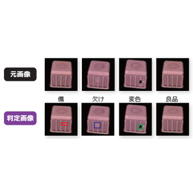
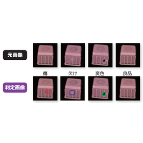
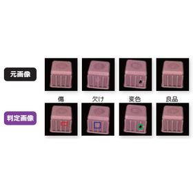
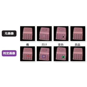
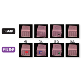
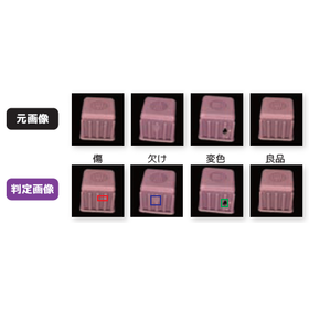
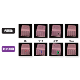
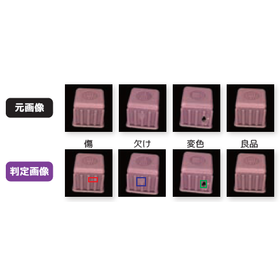
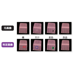
"NuLMiL" is an appearance inspection AI that can automatically classify defect types simply by learning to color-code the defective parts of images. The AI is trained with color-coded image data for each type of defect, allowing it to automatically detect and classify defects based on the colors it has learned. Based on the design philosophy of "equipment that anyone can use," we provide a one-stop solution to our customers' challenges with inspection devices that require minimal poka-yoke and setup effort. 【Features】 ■ Improved accuracy through A/B testing and autonomous learning ■ Support functions for undetected, over-detected, and misclassified defects, NG map ■ Additional features that address specific needs: - Alignment - Discharge coordination - Detection limits and resolution *For more details, please download the PDF or feel free to contact us.

Added to bookmarks

Bookmarks list

Bookmark has been removed

Bookmarks list

You can't add any more bookmarks

By registering as a member, you can increase the number of bookmarks you can save and organize them with labels.

Free membership registration

NuLMiL for Automobiles: AI Scratch Detection

Learn directly from defective samples! Automating scratch detection in automotive parts.

In the automotive industry, detecting scratches through visual inspection is crucial for product quality control. In particular, scratches on painted surfaces and molded parts can not only diminish the product's value but also potentially affect safety. Visual inspections can vary in accuracy depending on the inspector's skill level, and there is a risk of oversight. NuLMiL automatically detects and classifies defects simply by marking the defective areas, automating visual inspections based on inspection standards, and contributing to the efficiency and stability of quality control. 【Application Scenarios】 - Scratch detection on painted surfaces - Scratch detection on molded parts - Scratch detection during assembly processes 【Benefits of Implementation】 - Improved inspection accuracy - Reduced inspection time - Lower labor costs - Prevention of defective products from being released

Added to bookmarks

Bookmarks list

Bookmark has been removed

Bookmarks list

You can't add any more bookmarks

By registering as a member, you can increase the number of bookmarks you can save and organize them with labels.

Free membership registration

NuLMiL for electronic components

An AI that learns directly from defective samples! Automating foreign matter contamination inspection.

In the electronic components industry, thorough elimination of foreign matter is required to ensure product quality and reliability. Particularly in electronic components with fine parts and complex structures, the presence of foreign matter can lead to significant issues such as decreased product performance and failures. NuLMiL is an appearance inspection AI that can automatically classify defective types simply by distinguishing defective parts. It enables early detection of foreign matter and prompt responses, helping to prevent the outflow of defective products. 【Usage Scenarios】 - Foreign matter inspection on electronic component manufacturing lines - Inspections in product quality control departments 【Benefits of Implementation】 - Reduction in the occurrence rate of defective products due to foreign matter - Cost savings through automation of the inspection process - Improvement in product quality and customer satisfaction
Added to bookmarks

Bookmarks list

Bookmark has been removed

Bookmarks list

You can't add any more bookmarks

By registering as a member, you can increase the number of bookmarks you can save and organize them with labels.

Free membership registration

NuLMiL for Food: AI Shape Inspection

Learn directly from defective samples! Automating the inspection of food shapes.

In the food industry, inspecting for foreign object contamination and shape defects is crucial to ensure product quality and safety. Particularly as manufacturing lines become faster, relying solely on visual inspections can lead to oversights. NuLMiL contributes to improving inspection accuracy and efficiency by automatically detecting and classifying defects through AI, simply by marking the defective areas. 【Use Cases】 - Shape inspection of food products - Foreign object contamination inspection - Quality control on manufacturing lines 【Benefits of Implementation】 - Improved inspection accuracy - Reduced inspection time - Lower labor costs - Prevention of defective products from being released

Added to bookmarks

Bookmarks list

Bookmark has been removed

Bookmarks list

You can't add any more bookmarks

By registering as a member, you can increase the number of bookmarks you can save and organize them with labels.

Free membership registration

[For Pharmaceuticals] NuLMiL: Automating Packaging Quality Control

An AI that learns from defective samples to streamline visual inspection of pharmaceutical packaging.

In the pharmaceutical industry, accurate inspection of packaging is essential to ensure the quality and safety of products. Deficiencies in packaging can lead to contamination or deterioration of products, potentially adversely affecting patient health. NuLMiL automates visual inspection of pharmaceutical packaging by allowing AI to detect and classify defects simply by highlighting the defective areas, contributing to improved efficiency in quality control. 【Usage Scenarios】 - Pharmaceutical packaging lines - Inspection of foreign matter contamination, printing errors, damage, etc. 【Benefits of Implementation】 - Improved inspection accuracy - Reduced inspection time - Lower labor costs

Added to bookmarks

Bookmarks list

Bookmark has been removed

Bookmarks list

You can't add any more bookmarks

By registering as a member, you can increase the number of bookmarks you can save and organize them with labels.

Free membership registration

NuLMiL for Metalworking

An AI that learns directly from defective samples! Automating visual inspection of metal surfaces.

In the metal processing industry, early detection of surface defects is essential to maintain product quality. In particular, surface defects such as scratches, dents, and foreign matter adhesion not only impair the performance and appearance of products but can also lead to customer complaints. NuLMiL is an appearance inspection AI that can automatically classify defect types simply by highlighting the defective areas. By automating visual inspections, it achieves greater inspection efficiency and stabilizes quality. 【Usage Scenarios】 - Manufacturing processes of metal parts - Inspection processes after surface treatment - Quality inspection of final products 【Benefits of Implementation】 - Reduction of inspection time - Improvement of inspection accuracy - Prevention of defective products from being released - Reduction of inspection costs

Added to bookmarks

Bookmarks list

Bookmark has been removed

Bookmarks list

You can't add any more bookmarks

By registering as a member, you can increase the number of bookmarks you can save and organize them with labels.

Free membership registration

NuLMiL for Plastic Products

An AI that learns directly from defective samples! Automating visual inspection.

In the deburring process of plastic products, detecting burrs that affect product quality is crucial. Visual inspections can lead to variations in inspection accuracy due to the experience and abilities of the inspectors, resulting in issues such as the outflow of defective products due to oversight and decreased productivity due to excessive inspections. NuLMiL automatically detects and classifies defects using AI by simply marking the defective areas, achieving standardization and efficiency in inspections. 【Use Cases】 - Inspection in the deburring process of plastic products - Appearance inspection of products after molding - Reducing the burden on inspectors 【Benefits of Implementation】 - Improved inspection accuracy - Reduced inspection time - Prevention of defective product outflow

Added to bookmarks

Bookmarks list

Bookmark has been removed

Bookmarks list

You can't add any more bookmarks

By registering as a member, you can increase the number of bookmarks you can save and organize them with labels.

Free membership registration

NuLMiL for Ceramics

An AI that learns directly from defective samples! Automating crack inspection of ceramic products.

In the ceramic industry, early detection of cracks is crucial for maintaining product quality. Particularly in ceramic products subjected to high-temperature environments and heavy loads, the occurrence of cracks can lead to a decline in product performance or damage. Visual inspections may result in variations in inspection accuracy depending on the inspector's skill level. NuLMiL automatically detects and classifies cracks simply by marking defective areas. This achieves greater efficiency in inspections and stabilizes quality. [Usage Scenarios] - Crack inspection in the manufacturing process of ceramic products - Inspection tasks in quality control departments - Integration into manufacturing lines [Benefits of Implementation] - Improved inspection accuracy - Reduced inspection time - Lower labor costs - Prevention of defective products from being released Our Strength: As the Watanabe Shokai Group, founded in 1930, we provide optimal solutions tailored to our customers' needs. As a manufacturing trading company, we have grown alongside the IT society by offering high-quality products and services.

Added to bookmarks

Bookmarks list

Bookmark has been removed

Bookmarks list

You can't add any more bookmarks

By registering as a member, you can increase the number of bookmarks you can save and organize them with labels.

Free membership registration

[For Semiconductors] NuLMiL - AI Appearance Inspection

Learn directly from defective samples! Automating visual inspections based on inspection standards.

In the semiconductor industry, it is essential to accurately detect minute defects in product quality control. Appearance inspection utilizing pattern recognition technology is crucial for improving product yield. NuLMiL is an appearance inspection AI that can automatically classify defect types simply by highlighting defective areas. By automating visual inspections, it achieves greater efficiency and stability in quality. 【Usage Scenarios】 - Appearance inspection in semiconductor manufacturing processes - Defect detection using pattern recognition technology - Efficiency improvements through the automation of visual inspections 【Benefits of Implementation】 - Improved inspection accuracy - Reduced inspection time - Lower labor costs

Added to bookmarks

Bookmarks list

Bookmark has been removed

Bookmarks list

You can't add any more bookmarks

By registering as a member, you can increase the number of bookmarks you can save and organize them with labels.

Free membership registration

O-ring "Katon"

Ideal for sealing in harsh environments! Balancing reliability and cost efficiency.

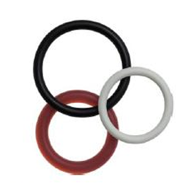
The O-ring "Katon" is a high-performance FFKM (perfluoroelastomer) and FKM O-ring seal product designed and manufactured by MAXMOLD. Thanks to its unique polymer filler technology, it achieves low metal release and contamination suppression. It has excellent resistance to strong acids, alkalis, solvents, and high-permeability gases, demonstrating stable performance even in extremely harsh environments such as high temperatures, vacuum, and high-purity processes. In critical sealing applications where long-term operation and wear resistance are required, it provides extended lifespan and high reliability, while also contributing to significant cost reductions. 【Features】 ■ Resistance to strong acids, alkalis, solvents, and high-permeability gases ■ Suitable for high temperatures, low contamination, vacuum, and high-purity processes ■ Long-term operation, wear resistance, and stable sealing performance ■ Development of unique high-purity FFKM compounds ■ Balancing reliability and cost efficiency *For more details, please download the PDF or feel free to contact us.

Added to bookmarks

Bookmarks list

Bookmark has been removed

Bookmarks list

You can't add any more bookmarks

By registering as a member, you can increase the number of bookmarks you can save and organize them with labels.

Free membership registration
Prev 1 Next
  • 令和8年度 ゼロエミ製品 開発助成金 電子申請 受付中 ゼロエミッションを推進する製品開発、改良、 規格等適合化に要する経費の一部を助成します。 助成金額 単独 1,500万円 共同 3,000万円
  • 金属・化学・窯業 食品・医薬品などの ほぐし・解砕 ふるい分けがこれ一台 解砕機構付き佐藤式振動ふるい機 つばさ デモ実施中!
    • Contact this company

      Inquiry Form

    Products

    • Search for Products

    Company

    • Search for Companies

    Special Features

    • Special Features

    Ranking

    • Overall Products Ranking
    • Overall Company Ranking

    support

    • site map
    IPROS
    • privacy policy Regarding external transmission of information
    • terms of service
    • About Us
    • Careers
    • Advertising
    COPYRIGHT © 2001-2026 IPROS CORPORATION ALL RIGHTS RESERVED.
    Please note that the English text on this page is automatically translated and may contain inaccuracies.