iPROS Manufacturing
  • Search for products by classification category

    • Electronic Components and Modules
      Electronic Components and Modules
      61393items
    • Machinery Parts
      Machinery Parts
      75583items
    • Manufacturing and processing machinery
      Manufacturing and processing machinery
      101686items
    • Scientific and Physics Equipment
      Scientific and Physics Equipment
      36141items
    • Materials
      Materials
      37636items
    • Measurement and Analysis
      Measurement and Analysis
      55311items
    • Image Processing
      Image Processing
      15314items
    • Control and Electrical Equipment
      Control and Electrical Equipment
      54240items
    • Tools, consumables, and supplies
      Tools, consumables, and supplies
      65270items
    • Design and production support
      Design and production support
      12646items
    • IT/Network
      IT/Network
      45266items
    • Office
      Office
      14106items
    • Business support services
      Business support services
      25178items
    • Seminars and Skill Development
      Seminars and Skill Development
      6528items
    • Pharmaceutical and food related
      Pharmaceutical and food related
      33515items
    • others
      74943items
  • Search for companies by industry

    • Manufacturing and processing contract
      7328
    • others
      4979
    • Industrial Machinery
      4433
    • Machine elements and parts
      3316
    • Other manufacturing
      2882
    • Trading company/Wholesale
      2596
    • IT/Telecommunications
      2553
    • Industrial Electrical Equipment
      2312
    • Building materials, supplies and fixtures
      1815
    • software
      1653
    • Electronic Components and Semiconductors
      1572
    • Resin/Plastic
      1499
    • Service Industry
      1459
    • Testing, Analysis and Measurement
      1129
    • Ferrous/Non-ferrous metals
      984
    • environment
      698
    • Chemical
      637
    • Automobiles and Transportation Equipment
      572
    • Printing Industry
      512
    • Information and Communications
      464
    • Consumer Electronics
      412
    • Energy
      326
    • Rubber products
      318
    • Food Machinery
      307
    • Optical Instruments
      277
    • robot
      272
    • fiber
      253
    • Paper and pulp
      228
    • Pharmaceuticals and Biotechnology
      170
    • Electricity, Gas and Water Industry
      165
    • Warehousing and transport related industries
      149
    • Glass and clay products
      139
    • Food and Beverage
      130
    • CAD/CAM
      123
    • retail
      108
    • Medical Devices
      105
    • Educational and Research Institutions
      103
    • Ceramics
      98
    • wood
      88
    • Transportation
      82
    • Petroleum and coal products
      62
    • Medical and Welfare
      61
    • Shipbuilding and heavy machinery
      50
    • Aviation & Aerospace
      47
    • Fisheries, Agriculture and Forestry
      41
    • equipment
      38
    • Public interest/special/independent administrative agency
      31
    • Materials
      28
    • Research and development equipment and devices
      27
    • Government
      24
    • self-employed
      24
    • Mining
      17
    • Finance, securities and insurance
      13
    • cosmetics
      13
    • Individual
      10
    • Restaurants and accommodations
      9
    • Police, Fire Department, Self-Defense Forces
      7
    • Laboratory Equipment and Consumables
      5
    • Raw materials for reagents and chemicals
      3
    • Contracted research
      3
  • Special Features
  • Ranking

    • Overall Products Ranking
    • Overall Company Ranking
Search for Products
  • Search for products by classification category

  • Electronic Components and Modules
  • Machinery Parts
  • Manufacturing and processing machinery
  • Scientific and Physics Equipment
  • Materials
  • Measurement and Analysis
  • Image Processing
  • Control and Electrical Equipment
  • Tools, consumables, and supplies
  • Design and production support
  • IT/Network
  • Office
  • Business support services
  • Seminars and Skill Development
  • Pharmaceutical and food related
  • others
Search for Companies
  • Search for companies by industry

  • Manufacturing and processing contract
  • others
  • Industrial Machinery
  • Machine elements and parts
  • Other manufacturing
  • Trading company/Wholesale
  • IT/Telecommunications
  • Industrial Electrical Equipment
  • Building materials, supplies and fixtures
  • software
  • Electronic Components and Semiconductors
  • Resin/Plastic
  • Service Industry
  • Testing, Analysis and Measurement
  • Ferrous/Non-ferrous metals
  • environment
  • Chemical
  • Automobiles and Transportation Equipment
  • Printing Industry
  • Information and Communications
  • Consumer Electronics
  • Energy
  • Rubber products
  • Food Machinery
  • Optical Instruments
  • robot
  • fiber
  • Paper and pulp
  • Pharmaceuticals and Biotechnology
  • Electricity, Gas and Water Industry
  • Warehousing and transport related industries
  • Glass and clay products
  • Food and Beverage
  • CAD/CAM
  • retail
  • Medical Devices
  • Educational and Research Institutions
  • Ceramics
  • wood
  • Transportation
  • Petroleum and coal products
  • Medical and Welfare
  • Shipbuilding and heavy machinery
  • Aviation & Aerospace
  • Fisheries, Agriculture and Forestry
  • equipment
  • Public interest/special/independent administrative agency
  • Materials
  • Research and development equipment and devices
  • Government
  • self-employed
  • Mining
  • Finance, securities and insurance
  • cosmetics
  • Individual
  • Restaurants and accommodations
  • Police, Fire Department, Self-Defense Forces
  • Laboratory Equipment and Consumables
  • Raw materials for reagents and chemicals
  • Contracted research
Special Features
Ranking
  • Overall Products Ranking
  • Overall Company Ranking
  • privacy policy
  • terms of service
  • About Us
  • Careers
  • Advertising
  1. Home
  2. Testing, Analysis and Measurement
  3. プレシテック・ジャパン
  4. Semicon Japan 2024
SEMINAR_EVENT
  • Aug 08, 2025
  • Added to bookmarks

    Bookmarks list

    Bookmark has been removed

    Bookmarks list

    You can't add any more bookmarks

    By registering as a member, you can increase the number of bookmarks you can save and organize them with labels.

    Free membership registration
Aug 08, 2025

Semicon Japan 2024

プレシテック・ジャパン プレシテック・ジャパン
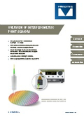
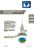
We will be exhibiting at Semicon Japan 2024, which will be held at Tokyo Big Sight from December 11 (Wednesday) to December 12 (Friday). If you are interested, please come to the venue. ■ Products to be exhibited 1. Spectral interference optical thickness sensor CHRocodile 2 DW/ 2IT 2. Area scanner for measuring the thickness and shape of 12" wafers - Flying Spot Scanner (FSS) 3. Chromatic aberration confocal optical line sensor CLS2.0 4. Chromatic aberration confocal line camera CVC 5. Chromatic aberration confocal optical single-point sensor CHRocodile Mini 6. Non-contact thickness measurement sensor for opaque materials Enovasnese 7. Sensor for detecting internal defects non-contactly - Field sensor
Date and time Wednesday, Dec 17, 2025 ~ Friday, Dec 19, 2025
10:00 AM ~ 05:00 PM
Capital Tokyo Big Sight East Hall 2, Booth Number #2305 ■ Exhibition Website https://www.semiconjapan.org/jp ■ Exhibition Visitor Registration https://semi.eventos.tokyo/web/portal/609/event/11724/users/login
Entry fee Free
  • Inquiry about this news

    Contact Us Online
  • More Details & Registration

    Details & Registration

Related product
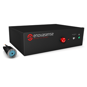
Enovasense 写真.PNG

Non-contact thickness measurement of opaque materials using laser photothermal sensors - case studies available.

For high-precision thickness measurement of opaque materials, Enovasense's laser photo-thermal sensor can measure thickness from a minimum of 10nm, regardless of the material.

The sensors from the French company Enovasense are high-performance sensors that use laser photothermal technology to measure the thickness of opaque materials non-contactly. ■Features - Non-contact measurement of the thickness of opaque materials is possible, eliminating the need for destructive testing. - A wide measurement range from a minimum of 10nm to a maximum of 1mm. - High precision measurements of 0.5% to 3% or less are achievable, recommended for those lacking accuracy. - Capable of measuring various combinations of materials regardless of the base material. ■Applications Used in a wide range of fields including the automotive industry, aerospace industry, consumer goods, industrial products, medical industry, and semiconductors, for various applications such as coating thickness, metal plating thickness, and paint film thickness. *Currently, Enovasense is a group company of the German optical sensor manufacturer Precitec. *For more details, please refer to the materials. Feel free to contact us with any inquiries.

  • Coating thickness gauge

Added to bookmarks

Bookmarks list

Bookmark has been removed

Bookmarks list

You can't add any more bookmarks

By registering as a member, you can increase the number of bookmarks you can save and organize them with labels.

Free membership registration
スクリーンショット 2024-06-05 113647.png

Non-contact small optical distance sensor [CHRocodile C/Mini]

Affordable distance sensors for measuring film and coating thickness, as well as non-contact thickness measurement. Strong performance on slopes, achieving a distance direction resolution of 20nm!

Our optical distance sensor/thickness sensor 'CHRocodile C / CHRocodile Mini' from PreciTech Japan is a compact non-contact sensor with a wide measurement range. It is robust against slopes and offers high resolution in the distance direction starting from 20nm, all at an affordable price of approximately 1 million yen (excluding tax). 【Examples of Use Cases】 ● Complete inspection through height and distance measurement of manufactured products within equipment ● Quality improvement through thickness management of glass, film, and graphite coatings ⇒ Adopted by manufacturers of production equipment, inspection equipment, and integrators. 【Features】 ・Combines high resolution with a price point that lowers the purchasing barrier ・Non-contact measurement of film and coating thickness ・Strong against slopes with an angle tolerance of up to ±45 degrees ・Distance direction resolution starting from 20nm ・Flexible software creation possible with the provided software development kit ・Can be embedded in equipment ・Compatible with rough and mirror surfaces, independent of surface or shape *For product details, please refer to the materials available for download in PDF format. Feel free to contact us for inquiries.

  • Distance measuring device

Added to bookmarks

Bookmarks list

Bookmark has been removed

Bookmarks list

You can't add any more bookmarks

By registering as a member, you can increase the number of bookmarks you can save and organize them with labels.

Free membership registration
Enovasenes field sensor.png

Enovasense Field Sensor

High-speed opaque film thickness mapping and area detection of internal defects using a laser photothermal sensor.

The sensors from the French company Enovasense are high-performance sensors that use laser photothermal technology to measure the thickness of opaque materials non-contactly. This new product is an area sensor that can simultaneously measure approximately 110,000 points, unlike conventional single-point sensors. It can detect not only the thickness mapping of opaque materials but also the presence of defects, chips, and delaminations beneath the surface layer. ■ Features - Non-contact measurement of the following: ☆ Thickness mapping of opaque materials ☆ Detection of defects beneath opaque surface material layers No destructive testing is required. - As an area sensor, it can measure approximately 110,000 points simultaneously in one second. - It can also be applied to detect defects in areas such as welds, where conventional X-ray or CT scans are typically required. - Measurement is possible with various combinations of materials, regardless of the base material. ■ Applications Automotive industry, aerospace industry, consumer goods, industrial products, medical industry, semiconductor field. It can be used in various applications such as coating thickness, metal plating thickness, paint films, and welds. *For more details, please check the PDF download or contact us.

  • Defect Inspection Equipment

Added to bookmarks

Bookmarks list

Bookmark has been removed

Bookmarks list

You can't add any more bookmarks

By registering as a member, you can increase the number of bookmarks you can save and organize them with labels.

Free membership registration
スクリーンショット 2024-03-01 124138.png

CHRocodile 2 SX Optical Wide-Range Thickness Measurement Sensor

Optical sensor for measuring a wide range of thickness from 0.5 to 200 um. High-speed sampling at 5 kHz. Ideal for monitoring applications during processing.

Non-contact optical thickness measurement. Applicable for thickness measurement of semiconductor wafers where high precision is required. The new product 'CHRocodile 2 SX' is a device that can measure the thickness of materials such as wafers and coatings without contact. It supports high-speed sampling of up to 5 kHz, making it suitable for inline applications. In addition to measuring the thickness of semiconductor wafers like Si, it can also measure the thickness of films, resins, glass, solar cells, and more. In particular, when thickness monitoring is desired during wafer grinding, it can measure thicknesses from 200 µm to 0.5 µm for Si wafers. 【Features】 ■ Wide range of thickness measurement, compatible with various materials With a rich lineup of probes, it can measure thicknesses from thin films (around 2 µm) to thick films (1000 µm) at optical lengths, and from 0.5 to 200 µm for Si. ■ High resolution (sub-micron, minimum 3 nm @ optical length) ■ Contributes to reducing development costs and shortening development lead times, with a software development kit (DLL, etc.) available for device integration ■ Extensive track record in the semiconductor industry *For more details, please refer to the documentation.

  • Coating thickness gauge

Added to bookmarks

Bookmarks list

Bookmark has been removed

Bookmarks list

You can't add any more bookmarks

By registering as a member, you can increase the number of bookmarks you can save and organize them with labels.

Free membership registration
FSS310.png

Optical Area Scanner Flying Spot Scanner 310

Capable of measuring the total thickness of 12-inch wafers. High-speed measurement without the influence of vibrations, without a scanning stage. Suitable for online, offline, and wafer inspection applications.

The Flying Spot Scanner 310 is an optical measuring device that can perform wide-area (up to φ310) scans using XY2-axis galvanometer mirrors. Since stage scanning is not required, there is no influence from vibrations of the stage. It can measure thickness, dimensional shapes, and inspect surface defects based on the principle of spectral interference. Additionally, due to the coaxial optical system for incident and reflected light, it is possible to obtain good results even on glossy surfaces. 【Features】 ■ Wide-area scan φ310mm ■ High resolution XY20um Beam spot diameter 40um, high Z resolution through spectral interference method ■ No XY stage required, no stage vibrations Area scanning using galvanometer mirrors ■ Reduced development costs and shortened development lead times Software development kit for device integration (DLL, etc.) available ■ Applications Thickness measurement of 12-inch wafer surfaces, thickness measurement of bonded wafers, void inspection *For more details, please refer to the documentation.

  • 3D measuring device
  • Coating thickness gauge

Added to bookmarks

Bookmarks list

Bookmark has been removed

Bookmarks list

You can't add any more bookmarks

By registering as a member, you can increase the number of bookmarks you can save and organize them with labels.

Free membership registration
2LR.png

Thickness measurement - Optical sensor 'CHRocodile 2LR ver2'

Non-contact optical thickness measurement. Applicable even for thickness measurements of semiconductor wafers where high precision is required.

The new product "CHRocodile 2LR ver2" is a device that can non-contact measure the thickness of materials such as wafers and coatings. It adopts a new detector different from the previous "CHRocodile 2LR," allowing for approximately twice the thickness measurement range and more precise measurements. It can also be applied inline, and the CHRocodile 2LR has a proven track record with many customers. It is capable of measuring the thickness of semiconductor wafers like Si, as well as films, resins, glass, and solar cells. It supports interference film thickness of up to 16 layers. 【Features】  ■ Wide thickness measurement range, compatible with various materials    With a rich lineup of probes, it covers thicknesses from thin films (around 32μm) to thick films (3900μm). (The high-precision measurement range is 16~1900μm with linearity of 0.35μm)  ■ High resolution (sub-micron, minimum 1nm)  ■ Contributes to reducing development costs and shortening development lead times,    with a software development kit (DLL, etc.) available for device integration  ■ Extensive track record in the semiconductor industry *For more details, please refer to the documentation.

  • Coating thickness gauge
  • Other inspection equipment and devices

Added to bookmarks

Bookmarks list

Bookmark has been removed

Bookmarks list

You can't add any more bookmarks

By registering as a member, you can increase the number of bookmarks you can save and organize them with labels.

Free membership registration
CHRocodile_CLS2.0_chromatic_line_sensor_product_image.JPG

3D Line Sensor CHROCODILE CLS2 Series

Non-contact line sensor CLS. High precision, high speed, and wide range 3D shape measurement. High tolerance for angles suitable for edges and slopes. Numerous achievements in wafer edge measurement.

The "CHROCODILE CLS2" and "CHROCODILE CLS2 PRO" can achieve non-contact high-speed three-dimensional shape measurement at a maximum of 48 million points per second (standard is 16.8 million points per second). The resolution is also extremely high, with a maximum of Y1um and Z0.025um, allowing for very precise measurements. Compared to previous generations, there has been a significant reduction in measurement time, and improvements have been made for high NA and increased light volume suitable for wafer edges, wire bonding, and micro bump measurements. There are numerous applications including shape, surface roughness, step height (thickness), flatness, and TTV. It is suitable not only as a tabletop device but also for use as a sensor for in-situ, monitoring, and inline equipment integration. 【Features】 - Three-dimensional shape measurement over a wide area Maximum line width of 20mm - Wide tolerance angle Can accommodate ±53° on reflective surfaces, suitable for edges and steep slopes - Contributes to reduced development costs and shortened development lead times, with a compact unit and a software development kit for equipment integration (such as DLLs) also available - Rich track record across multiple industries Semiconductor industry, consumer electronics, glass manufacturing, medical field *For more details, please refer to the documentation.

  • 3D measuring device

Added to bookmarks

Bookmarks list

Bookmark has been removed

Bookmarks list

You can't add any more bookmarks

By registering as a member, you can increase the number of bookmarks you can save and organize them with labels.

Free membership registration
2020-01-16_13h41_08.png

Control of CMP processes and grinding processes in the semiconductor industry.

The "CHRocodile 2 IT sensor" can measure the thickness of wafers during work processing.

In the semiconductor industry, it is necessary to measure the physical thickness of wafers at multiple manufacturing stages, such as CMP and mechanical grinding. To monitor and optimize the entire process, it is important to have a grasp of the thickness; however, this task is currently mainly performed using mechanical contact probes. These probes have significant drawbacks, including the need for contact with the wafer, surface damage, and reference values for thickness measurement from the chuck table, and they also wear out, necessitating frequent replacements. Our "CHRocodile 2 IT sensor" can measure the thickness of wafers during processing using non-contact, non-destructive optical measurement technology. 【Features】 - Optical sensor provides more accurate results than conventional contact measurement devices. - Direct feedback improves the reproducibility of wafer thickness from several micrometers to less than 0.5 micrometers. - High-speed measurement and non-contact passive probes allow for the acquisition of a large amount of thickness data across the entire wafer area simply by moving the probe over the sample. - Variability in wafer thickness is revealed from the results, enabling the management of variability during the grinding process. *Product details can be viewed in the materials available for download in PDF format.

  • Sensors

Added to bookmarks

Bookmarks list

Bookmark has been removed

Bookmarks list

You can't add any more bookmarks

By registering as a member, you can increase the number of bookmarks you can save and organize them with labels.

Free membership registration
image.jpg

Thickness measurement - Optical sensor 'CHRocodile 2DW series'

Use an appropriate light source wavelength for doped wafers to accommodate challenging doped wafer thickness measurements.

The "CHRocodile 2DW Series" is a device that can non-contact measure the thickness of materials such as wafers and coatings. It is capable of measuring doped wafers and can be applied in-line, with a proven track record among many customers. In addition to measuring the thickness of semiconductor wafers like sapphire, Si, and SiC, it can also measure the thickness of films, resins, glass, and solar cells. It supports interference film thickness of up to 16 layers. 【Features】  ■ Wide range of thickness measurement, compatible with various materials    With a rich lineup of probes, it covers thickness from thin films (a few micrometers) to thick films (780 micrometers). It supports doped wafers.  ■ High resolution (sub-micron, minimum 1nm)  ■ Contributes to reducing development costs and shortening development lead times,    with a software development kit (DLL, etc.) available for device integration  ■ Extensive track record in the semiconductor industry *For more details, please refer to the documentation. Feel free to contact us with any inquiries.

  • Other measurement, recording and measuring instruments
  • Sensors

Added to bookmarks

Bookmarks list

Bookmark has been removed

Bookmarks list

You can't add any more bookmarks

By registering as a member, you can increase the number of bookmarks you can save and organize them with labels.

Free membership registration
MIRA.png

SEMI-compliant 12-inch wafer thickness and shape measurement system

12" wafer full inspection accelerated, can also be used for full inspection of wafers.

The TTV, Bow, and Warp measurements of the entire wafer can be performed. With a measurement speed of up to 70,000 points per second, it is possible to measure the entire surface in about 2 minutes with a pitch of 160 µm in the XY direction. This is a full system equipped with software compliant with SEMI standards. The sensors used can be selected from our spectral interference sensor 2IT DW series, allowing for high-precision measurements with a Z resolution of 1 nm or better. The high-speed measurement of the entire wafer is made possible by our area scanner FSS310, which is incorporated into the system.

  • Coating thickness gauge

Added to bookmarks

Bookmarks list

Bookmark has been removed

Bookmarks list

You can't add any more bookmarks

By registering as a member, you can increase the number of bookmarks you can save and organize them with labels.

Free membership registration
2S.png

Optical single-point sensor using chromatic aberration confocal method

Embedded optical sensor for high-precision and high-speed measurement of thickness and shape.

This is a single-point sensor using a chromatic aberration confocal method from Pretech, characterized by high precision and high-speed measurement. It has a proven track record in reducing measurement time for thickness and shape, as well as in full inspection. Due to the chromatic aberration confocal method, it is also possible to use probes with a large angular tolerance. There is also a budget sensor lineup available, starting from approximately 800,000 yen. *For more details, please refer to the materials. Feel free to contact us as well.*

  • Distance measuring device

Added to bookmarks

Bookmarks list

Bookmark has been removed

Bookmarks list

You can't add any more bookmarks

By registering as a member, you can increase the number of bookmarks you can save and organize them with labels.

Free membership registration

Related catalog(10)

Doppler wafer measurement - High-speed and high-precision measurement using a non-contact optical sensor.

Doppler wafer measurement - High-speed and high-precision measurement using a non-contact optical sensor.

APPLICATION_NOTE
  • E-book viewing
  • Catalog download

Contact this catalog

Data Sheet Spectral Interference Sensor Version 20250423

Data Sheet Spectral Interference Sensor Version 20250423

PRODUCT
  • E-book viewing
  • Catalog download

Contact this catalog

Data Sheet Color Aberration Confocal Sensor Version 20250522

Data Sheet Color Aberration Confocal Sensor Version 20250522

PRODUCT
  • E-book viewing
  • Catalog download

Contact this catalog

Distance/Shape Measurement - Presitech Chromatic Aberration Confocal Sensor

Distance/Shape Measurement - Presitech Chromatic Aberration Confocal Sensor

PRODUCT
  • E-book viewing
  • Catalog download

Contact this catalog

Data Sheet: High-Speed Full Wafer Measurement System for 12" Wafers

Data Sheet: High-Speed Full Wafer Measurement System for 12" Wafers

DOCUMENT
  • E-book viewing
  • Catalog download

Contact this catalog

Introduction to Products and Applications of Color Aberration Confocal 3D Line Sensors

Introduction to Products and Applications of Color Aberration Confocal 3D Line Sensors

APPLICATION_NOTE
  • E-book viewing
  • Catalog download

Contact this catalog

High-power light source equipped CHRocodile 2S HP - Thickness measurement/Shape measurement

High-power light source equipped CHRocodile 2S HP - Thickness measurement/Shape measurement

APPLICATION_NOTE
  • E-book viewing
  • Catalog download

Contact this catalog

Non-contact small single-point sensors 'CHRocodile C' and 'CHRocodile Mini'

Non-contact small single-point sensors 'CHRocodile C' and 'CHRocodile Mini'

PRODUCT
  • E-book viewing
  • Catalog download

Contact this catalog

Presitech CHRocodile Sensor Lineup Spectral Interference Thickness Measurement

Presitech CHRocodile Sensor Lineup Spectral Interference Thickness Measurement

PRODUCT
  • E-book viewing
  • Catalog download

Contact this catalog

New Product - CHRocodile 2 SX Optical Wide-Range Thickness Measurement Sensor

New Product - CHRocodile 2 SX Optical Wide-Range Thickness Measurement Sensor

PRODUCT
  • E-book viewing
  • Catalog download

Contact this catalog

Distributors

プレシテック・ジャパン
Testing, Analysis and Measurement
  • Added to bookmarks

    Bookmarks list

    Bookmark has been removed

    Bookmarks list

    You can't add any more bookmarks

    By registering as a member, you can increase the number of bookmarks you can save and organize them with labels.

    Free membership registration
プレシテック・ジャパン
  • Special site
  • Official site
Phone number/address

news

[Notice of Exhibition Participation by Fukuda Co., Ltd.] __th Measurement and Measurement Exhibition INTERMEASURE 202_

  • NEW
  • SEMINAR_EVENT

We would like to express our congratulations on the continued prosperity of your esteemed company. Our company will be exhibiting at the following trade show, where we will introduce a number of products, including new ones. We sincerely apologize for the inconvenience during your busy schedule, but we would like to invite you to attend this event. 【 Exhibition Name 】 31st Measurement and Measurement Exhibition INTERMEASURE 2024 Official Website: https://intermeasure.org/itms2024/ 【 Dates 】 From __ (Wednesday) to __ (Friday), 202_ 【 Venue 】 Tokyo Big Sight (Tokyo International Conference Center) East Hall (Booth Number: ___) 【 Exhibited Products 】 - Air Leak Tester - Hydrogen Leak Detector - Pin Hole (Reference Test Piece) and more. For more details, please refer to the "Related Materials" (PDF file) below.

Aug 19, 2026

Added to bookmarks

Bookmarks list

Bookmark has been removed

Bookmarks list

You can't add any more bookmarks

By registering as a member, you can increase the number of bookmarks you can save and organize them with labels.

Free membership registration

■Notice of Participation in "H₂ & FC EXPO Spring International Hydrogen and Fuel Cell Exhibition"■【February 28 (Wednesday) - March 1 (Friday), 2024】

  • NEW
  • SEMINAR_EVENT

Nitto Kohki will exhibit at the "H₂ & FC EXPO Spring International Hydrogen and Fuel Cell Exhibition" held at Tokyo Big Sight, West Exhibition Hall 2, from February 28 (Wednesday) to March 1 (Friday), 2024. [Booth Number: W14-63] The quick fluid coupling "Coupler" is a product that allows for the rapid connection and disconnection of piping for various fluids such as air, water, oil, and chemical solutions. At this exhibition, we will primarily showcase the high-pressure hydrogen filling quick fluid coupling "HHV Coupler."

Aug 17, 2026

Added to bookmarks

Bookmarks list

Bookmark has been removed

Bookmarks list

You can't add any more bookmarks

By registering as a member, you can increase the number of bookmarks you can save and organize them with labels.

Free membership registration

Next-generation CFD post-processor "EPPIC" product introduction seminar

  • NEW
  • SEMINAR_EVENT

☆☆☆ Urgent Visit to Japan & Emergency Event Announcement ☆☆☆ Dr. Yuval Levy, CEO of ISCFDC and developer of EPPIC, who has been involved in CFD research at NASA Ames Research Center for about five years, is coming to Japan! He will demonstrate and explain advanced CFD technologies, application cases, and the latest features of EPPIC himself. □ Date and Time □ July 31, 2026 (Friday) 13:00-18:00 (Registration starts at 12:30) <Part 1: Post-Processor Session> 13:00-16:40 <Part 2: Pre-Processor Session> 16:50-17:50 <Networking Event> 18:10-19:40 □ For more details □ Visit the Hulinks page https://www.hulinks.co.jp/seminar/eppic/

Aug 17, 2026

Added to bookmarks

Bookmarks list

Bookmark has been removed

Bookmarks list

You can't add any more bookmarks

By registering as a member, you can increase the number of bookmarks you can save and organize them with labels.

Free membership registration
Alliance iS HPLC System

"One Rank Higher LC Application Seminar" to Help Improve Analysis Accuracy - A Total of 6 Sessions Held [Live Webinar]

  • NEW
  • SEMINAR_EVENT

[Viewer Benefits Available] Explaining Tips for LC in a Short Seminar Do you have concerns such as "I'm unsure about column selection," "I'm struggling to optimize analysis conditions," or "I have challenges analyzing compounds with weak retention" in LC analysis? Waters will hold a seminar titled "Must-Listen! Advanced LC Application Seminar" where you can learn practical LC analysis know-how in just 30 minutes. In this seminar, we will cover useful topics in a total of six sessions, including tips for choosing detectors, how to utilize reverse phase columns, scaling up to preparative LC, approaches for analyzing hydrophilic and highly polar compounds, case studies of low-adsorption HPLC, and improving purity through solid-phase extraction. Each session is scheduled to start at 15:00. Event Themes: • October 6 (Tuesday) - Session 1: Tips for Choosing Detectors • October 13 (Tuesday) - Session 2: Tips for Choosing Columns • October 21 (Wednesday) - Session 3: Tips for Preparative LC • October 27 (Tuesday) - Session 4: Approaches for Analyzing Hydrophilic and Highly Polar Compounds • November 5 (Tuesday) - Session 5: Case Studies of Low-Adsorption HPLC • November 10 (Tuesday) - Session 6: Tips for Solid-Phase Extraction

Aug 17, 2026

Added to bookmarks

Bookmarks list

Bookmark has been removed

Bookmarks list

You can't add any more bookmarks

By registering as a member, you can increase the number of bookmarks you can save and organize them with labels.

Free membership registration

<Online Seminar> High-Confidence Proteome Analysis Achieved with Limited Plasma Volume

  • NEW
  • SEMINAR_EVENT

In liquid biopsy research, we will introduce a technical evaluation of proteome analysis to obtain reliable data from trace plasma, as well as case studies on data quality verification using the Contamination Index and Simple Western.

Aug 17, 2026

Added to bookmarks

Bookmarks list

Bookmark has been removed

Bookmarks list

You can't add any more bookmarks

By registering as a member, you can increase the number of bookmarks you can save and organize them with labels.

Free membership registration
Return to news list
  • ダマになりやすい原料も1台で解砕ふるい分け カスタマイズ可能な回転羽根形状で様々な原料に対応! 解砕機構付き佐藤式振動ふるい機つばさ 活用イメージ動画を公開中!
  • あなたの設計時間 CADに奪われていませんか? 制約から解放される新たな設計環境へ
    • Inquiry about this news

      Contact Us Online
    • More Details & Registration

      Details & Registration

    Products

    • Search for Products

    Company

    • Search for Companies

    Special Features

    • Special Features

    Ranking

    • Overall Products Ranking
    • Overall Company Ranking

    support

    • site map
    IPROS
    • privacy policy Regarding external transmission of information
    • terms of service
    • About Us
    • Careers
    • Advertising
    IPROS Services
    • >IPROS GMS | Search site for the manufacturing industry
    • >IPROS | Search site for the B2B industry
    COPYRIGHT © 2001-2026 IPROS CORPORATION ALL RIGHTS RESERVED.
    Please note that the English text on this page is automatically translated and may contain inaccuracies.