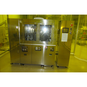
Research and development small-sized developer SPD40
【Process】Input → Development → Liquid Cutting → Circulating Water Wash → Direct Water Wash → Squeezing → Extraction 【Substrate Size】Max. W400×L500mm Thickness 0.4-2.0mm 【Nozzle Swing】Horizontal Swing 【Device Size】W1300×L1590×H1215mm - Space-saving for research use - Ideal for material development and testing - Capable of developing PCBs and LCDs

Inquire About This Product
basic information
◆ High-precision development is possible with a nozzle arrangement that accommodates fine patterns through horizontal oscillation. ◆ Can be installed in narrow spaces. ◆ User-friendly features and a sleek design. ◆ Affordable entry-level model. ◆ Short delivery times are possible due to standard specifications. ◆ Customization is possible according to specifications. ◆ Compatible with various development solutions.
Price information
4 to 4.5 million yen (price of the equipment itself)
Price range
P5
Delivery Time
※2.5 to 3 months
Applications/Examples of results
◆Conditions before setting up the mass production line ◆Evaluation and research of materials and chemicals ◆Basic research and development ◆Quality control ◆Small-scale production
Company information

◆Development, etching, stripping devices/cleaning devices for FPC ◆Development, etching, stripping devices/cleaning devices for COF ◆Development, etching, stripping devices/cleaning devices for FPD (TFT/PDP) ◆Cleaning devices for solar cells ◎Fine technology Fine results cannot be reproduced without a comprehensive design that combines nozzle arrangement, nozzle characteristics, oscillation, pressure adjustment, etc. ◎Thin plate transport technology Experience and proven results are essential for transporting thin plates without damage. The Ninomiya system has incorporated creativity and ingenuity to achieve reliable transport. ◎High reliability Devices designed to achieve a higher level can be used with confidence by our customers. The Ninomiya system does not compromise on device manufacturing.


![[Coating Success Case] Eliminate Line Troubles with Durable Surface Treatment!](https://image.mono.ipros.com/public/product/image/d44/2000232758/IPROS63798675243663290207.jpeg?w=280&h=280)
![[Experimental Video] Experiment of Film Attachment Using Static Electricity!](https://image.mono.ipros.com/public/product/image/aa8/2000260954/IPROS89350892149731541416.png?w=280&h=280)
![[Case Presentation] Process Improvement with Surface Treatment Technology to Enhance Release and Slipperiness](https://image.mono.ipros.com/public/product/image/0d7/2000666386/IPROS71675042821644158783.png?w=280&h=280)
