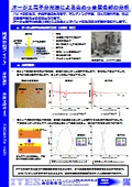
Non-destructive depth analysis of thin films on the nm order is possible! We will also introduce analysis examples.
At Aites Co., Ltd., we conduct depth profile analysis of thin film layers using angle-resolved XPS. By changing the angle between the sample and the XPS photoelectron detector, it is possible to vary the detection depth of the photoelectrons. The data obtained from this is numerically analyzed through simulation and converted into a depth profile. We achieve depth profile analysis of uniform thin films in the nanometer order near the surface, which is difficult to measure using conventional ion etching methods. We also have examples of analyzing the depth profile of HDD magnetic surfaces. 【Features】 ■ Non-destructive depth profile analysis of thin films in the nanometer order is possible ■ Achieves depth profile analysis of uniform thin films *For more details, please refer to the PDF document or feel free to contact us.

Inquire About This Product
basic information
For more details, please refer to the PDF document or feel free to contact us.
Price range
Delivery Time
Applications/Examples of results
For more details, please refer to the PDF document or feel free to contact us.
catalog(9)
Download All Catalogs


News about this product(1)

Company information

Aites was established in 1993, originating from the quality assurance department of the IBM Japan Yasu office. Based on the technical expertise cultivated through cutting-edge defect analysis and reliability assurance of electronic components at the IBM Japan Yasu office, we have provided various products and services that support the development and manufacturing of semiconductors, displays, organic EL, solar cells, and electronic components to customers both domestically and internationally.

![[Analysis Case] Evaluation of Layer Structure and Film Thickness of Naturally Oxidized Copper (Cu) Surface Film](https://image.mono.ipros.com/public/product/image/321/2000246635/IPROS13899729595871211119.png?w=280&h=280)


![Partial Discharge Online Remote Diagnosis Service [High Voltage Cable Diagnosis Without Power Interruption]](https://image.mono.ipros.com/public/product/image/2066136/IPROS9863170782217792517.png?w=280&h=280)