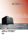
Thermal Microscope/TM3 Thin Film, Micro Area Thermal Conductivity Measurement
TM3
For evaluating thermal conductivity in thin films and micro-regions such as fillers, ceramics, insulating thin films, and semiconductor thin films!
This device is an innovative thermal property measurement instrument that boasts world-class minimal resolution. It can measure the thermal properties of samples in detail at the point, line, and surface levels, accurately capturing thermal property value distributions on the micron order that were difficult to achieve with conventional devices. Furthermore, this device realizes high resolution while being a non-contact measurement tool, pioneering areas that were previously impossible with traditional technology. Equipped with the world's first technology, it can directly measure thermal conductivity under favorable conditions in addition to measuring thermal diffusivity. This device demonstrates unparalleled performance in situations requiring precise thermal property analysis in research and development. 〇 About the Measurement Principle 〇 The measurement principle of this device is based on the thermoreflectance method. This is one of the techniques for measuring the surface temperature of materials with high precision, particularly used to investigate the thermal characteristics of micro-regions and thin film materials. This method detects changes in reflectivity associated with changes in the surface temperature of the material and measures the temperature from those changes. The results obtained are expressed as the parameter known as thermal diffusivity. Thermal diffusivity is a physical quantity that indicates how much heat is absorbed when two substances are in contact. It can be mutually converted into thermal conductivity and thermal diffusivity based on specific heat and density.

Inquire About This Product
basic information
【Features】 ○ High-resolution measurement of thermal properties in small areas (point, line, surface measurement) is possible with a detection light spot diameter of 3μm. ○ Non-contact measurement using a semiconductor laser. ○ By performing periodic heating, measurements can be taken at varying depths, allowing for analysis from thin films and multilayer films to bulk materials. ○ Samples on substrates can also be measured. ○ Detection of cracks, voids, and delamination beneath thin films is possible. ● For other functions and details, please contact us.
Price information
Please feel free to contact us.
Delivery Time
※Please feel free to contact us.
Applications/Examples of results
【Applications】 SiC, GaN, SiO2, DLc, Low-k films, various fillers, polyimide, various metals, etc. ● For other functions and details, please contact us.
catalog(4)
Download All Catalogs![[Company Information] Light, Heat, Safety, and Security / Bethel Corporation](https://image.mono.ipros.com/public/catalog/image/01/bb4/757276/IPROS75443977673002953408.jpeg?w=120&h=170)


News about this product(3)


Company information

Leveraging the assembly technology cultivated over many years, we have expanded our business areas to include the development of precision component assembly, thermal property measurement devices, contract measurement services, and the development of medical and dental plastic products equipped with clean rooms. We deepen and integrate our "original products" from a unique manufacturing perspective, consolidating our know-how and technology. With "speedy decision-making and execution," which is a strength unique to Bethel, we provide high-quality products under the "Made by BETHEL" label. Our wish at Bethel is for our customers who use Bethel products to be satisfied with our products, manufacturing, and services, and to feel that they made the right choice in trusting our company. Furthermore, we hope that the satisfaction of our customers will lead to the happiness of each employee who works here.


