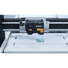
Semiconductor inspection sensor | Shape, thickness, and position measurement
SinceVision (Deep Vision Intelligence) / SR・SRI Series and others

For measuring the flatness and thickness of wafers, the coplanarity of BGAs, and the transport position. Here are examples from the semiconductor process.
We introduce measurement and inspection applications in semiconductor processes using SinceVision's 3D laser profilers, laser displacement sensors, spectral confocal displacement sensors, and transmission edge measurement sensors. Applications include measuring package flatness and parallelism, BGA solder ball coplanarity, wafer warpage, thickness, edge position, displacement of transport robots, and height measurement during dispensing. Depending on the measurement target and process, we select different sensor types and models. Please utilize this information to address on-site challenges such as shape acquisition of highly reflective surfaces and height measurement in limited installation spaces. If you provide us with the measurement target, required accuracy, takt time, and installation conditions, we can discuss configurations tailored to your applications.
Inquire About This Product
basic information
【Main Specifications and Application Values】 ■SRI8060 / 3D Laser Profiler Frame Rate: 67kHz, Flatness Measurement Error: <5μm ■SR7080 / 3D Laser Profiler Repeatability: Z-axis 0.4μm, X-axis 5μm, Inspection Speed: 150mm/s ■SRI8020 / 3D Laser Profiler Wafer Warpage Measurement Error: <5μm ■SD33 Series / Laser Displacement Sensor Lens Height Measurement Error: <8μm, Output/Communication: Analog/RS485 ■SD22 Series / Laser Displacement Sensor Body Dimensions: 44×20×25mm, Displacement Measurement Error: <0.01mm ■Spectral Confocal Displacement Sensor Flatness Measurement Accuracy: 1μm, Sampling Frequency: 33kHz (Flatness Measurement Example) ■Transmissive Edge Measurement Sensor Center Position Deviation: ±0.05mm, Angle Deviation: ±0.1° *The values listed are based on application-specific examples published by the manufacturer. They may vary depending on the applicable models, configurations, and measurement conditions.
Price range
Delivery Time
Applications/Examples of results
**Wafer Quality Control** - Measurement of flatness and warpage - Non-contact thickness measurement - Measurement of the outer ring height of TAIKO wafers **Inspection of Packaging and Assembly Processes** - Measurement of the flatness and parallelism of both sides of the package - Measurement of coplanarity of BGA solder balls - Measurement of height during the application of small amounts of adhesive and solder paste **Position and Height Management of Manufacturing Equipment** - Measurement of lens height in exposure equipment - Analysis of displacement deviation in X, Y, and Z directions of transport robots - Measurement of robot height through the glass of vacuum chambers - Edge detection and alignment of wafers For measurement methods and sensor characteristics by application, please refer to the illustrations below.
Detailed information
-
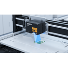
Measure the flatness and parallelism of packages quickly. The 3D laser profiler SRI8060 evaluates the flatness of the package and the parallelism of both top and bottom surfaces. It captures contours with a blue laser and can be used for shape verification before assembly. It supports a frame rate of 67 kHz and one-touch profile calibration. *The image is an illustration of the measurement configuration.
-
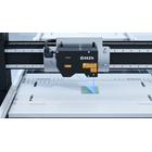
Even solder balls with strong reflections can be evaluated in 3D for height. The SR7080 utilizes optical design to minimize the effects of surface reflection on solder balls and obtain 3D shapes. It measures height variation and coplanarity of BGAs. There are examples of inspection speeds of 150mm/s, making it suitable for inspections on production lines. One-touch search for solder ball positions is also possible. *The image is an illustration of the measurement configuration.
-
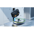
Measuring the height and warpage of wafers, which is difficult to capture in 2D images. The SRI8020 measures the height of the outer ring of TAIKO wafers and the warpage of the wafers. It captures the shape in the height direction, providing necessary information for depth management in the ring cutting process. By evaluating minute height differences, it supports shape confirmation before processing. *The image is an illustration of the measurement configuration.
-
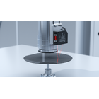
"Capturing lens height for interval management in the exposure process" The SD33 series laser displacement sensor measures the lens height of the exposure device in real-time. It obtains the data necessary for adjusting the distance between the lens and the wafer. It supports analog output and RS485, allowing you to choose the connection method according to the specifications of the device. *The image is an illustration of the measurement configuration.*
-
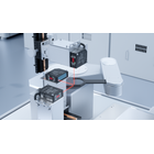
Using a small sensor to capture the minute positional deviations of a robot. The SD22 series, with dimensions of 44×20×25mm, is used. In the limited installation space around the robot, position data in the X, Y, and Z directions is obtained, and displacement deviations are analyzed. By combining the necessary sensor arrangements and quantities for each direction, it can be utilized for alignment evaluation. *The image is an illustration of the measurement configuration.
-
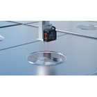
"Measuring the height of the robot from outside the vacuum chamber" Using a laser displacement sensor, the displacement of the internal robot is obtained through the glass of the chamber. This configuration allows for height verification from the outside while maintaining a vacuum state. Please consult us regarding applicable models and measurement configurations based on the material, thickness, and installation conditions of the glass. *The image is an illustration of the measurement configuration.*
-
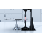
Measure thickness without touching the wafer. Thickness is measured using a spectral confocal method, avoiding the impact on the surface from contact probes. There are cases with a thickness measurement accuracy of 1μm, which can be utilized for thickness management within the process. This measurement method has low temperature drift, supporting stable measurements in production environments with temperature variations. *The image is an illustration of the measurement configuration.
-
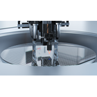
"With a small diameter head, capturing the height during micro-application" Measures the height of the work surface using a spectral confocal displacement sensor with a head diameter of 16mm. It accommodates materials with different reflective properties, such as metals, silicon wafers, and photoresists. It can be installed in limited spaces and supports height adjustment during the application of micro adhesives and solder pastes. *The image is an illustration of the measurement configuration.*
-
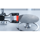
"Capture the edges of translucent wafers and utilize them for alignment." Detect the outer circumference of the wafer with a transmissive edge measurement sensor and measure the deviations in center position and angle. It supports edge detection of translucent materials and acquires the positional information necessary for the transport and alignment processes. With a sampling frequency of 4kHz, it supports position management on the production line. *The image is an illustration of the measurement configuration.*
Company information

SinceVision, established in 2014, is a manufacturer that provides industrial sensing and imaging technologies. We engage in research, development, manufacturing, and sales of industrial sensors, high-speed imaging systems, and high-sensitivity cameras. Our main products include 3D laser profilers, high-speed cameras, laser displacement sensors, spectral confocal displacement sensors, color sensors, transmission edge sensors, and sCMOS cameras. Our products are utilized in a wide range of fields, including automotive, lithium-ion batteries, semiconductors, electronics, solar power generation, and scientific research. Our technologies are employed in manufacturing sites around the world, including companies like Apple, Tesla, Samsung, LG, CATL, BYD, and Foxconn. Additionally, as a supporting member of the Japan Industrial Imaging Association (JIIA), we are also involved in the development and standardization activities in the field of industrial imaging and machine vision. Through high-precision measurement and inspection technologies, we contribute to improving product quality, automating inspection processes, enhancing production efficiency, and reducing costs.