1~4 item / All 4 items
Displayed results
Added to bookmarks
Bookmarks listBookmark has been removed
Bookmarks listYou can't add any more bookmarks
By registering as a member, you can increase the number of bookmarks you can save and organize them with labels.
Free membership registrationContact this company
Inquiry Form1~4 item / All 4 items
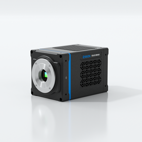
I want to capture the weak fluorescence of plant cells. I want to minimize the burden on the sample from the excitation light. The "Solis-B0465" from SinceVision is a back-illuminated sCMOS camera that meets these observation needs. ■ Efficient detection of weak fluorescence Equipped with a sensor that has a quantum efficiency of 95% (560nm). It captures weak fluorescence signals and supports observation with reduced excitation light. ■ Observe details with low noise Readout noise of 1.1e⁻ (median). Suitable for capturing weak signals. ■ Reduced dark current through cooling Adopts multi-stage TEC cooling and vacuum-sealed structure. It suppresses dark current during long exposures, supporting fluorescence imaging of plant cells. Please contact us regarding connection to microscopes and shooting conditions.
Added to bookmarks
Bookmarks listBookmark has been removed
Bookmarks listYou can't add any more bookmarks
By registering as a member, you can increase the number of bookmarks you can save and organize them with labels.
Free membership registration
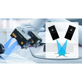
Capture the gaps around lamps and windows in 3D. This is a gap and step measurement solution for vehicle bodies using the SinceVision 3D laser profiler SR8060H. ■ Capture the edges of transparent parts Acquire the surface shape of transparent components such as lamps and glass. It supports gap measurement for parts with different optical properties than painted surfaces. ■ Reduce blind spots with two measurement heads Measure deep gaps and curved surfaces with measurement heads tilted face-to-face. It compensates for contours that are difficult to capture from a single direction, evaluating gap width and steps. ■ Visualize inspection conditions and record results Check the judgments for each measurement point on the screen and automatically generate inspection reports. By collaborating with system integrators, it supports the automation of vehicle body inspections.
Added to bookmarks
Bookmarks listBookmark has been removed
Bookmarks listYou can't add any more bookmarks
By registering as a member, you can increase the number of bookmarks you can save and organize them with labels.
Free membership registration
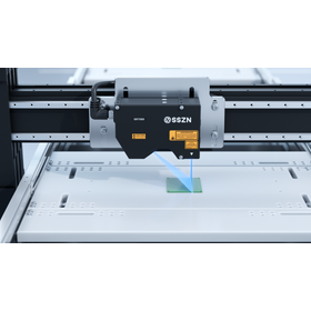
We introduce measurement and inspection applications in semiconductor processes using SinceVision's 3D laser profilers, laser displacement sensors, spectral confocal displacement sensors, and transmission edge measurement sensors. Applications include measuring package flatness and parallelism, BGA solder ball coplanarity, wafer warpage, thickness, edge position, displacement of transport robots, and height measurement during dispensing. Depending on the measurement target and process, we select different sensor types and models. Please utilize this information to address on-site challenges such as shape acquisition of highly reflective surfaces and height measurement in limited installation spaces. If you provide us with the measurement target, required accuracy, takt time, and installation conditions, we can discuss configurations tailored to your applications.
Added to bookmarks
Bookmarks listBookmark has been removed
Bookmarks listYou can't add any more bookmarks
By registering as a member, you can increase the number of bookmarks you can save and organize them with labels.
Free membership registration
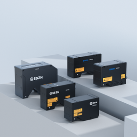
SinceVision's inline 3D profile measurement device measures the height, width, steps, gaps, flatness, contour shapes, and more of objects non-contactly using laser triangulation. It supports high-speed scanning up to 67kHz, with a maximum of 6400 points on the X-axis and a minimum repeatability accuracy of 0.1μm on the Z-axis, allowing for the acquisition of high-density 3D data even on high-speed transport lines. It can be utilized for the automation of inline inspection, dimensional measurement, and appearance inspection in various manufacturing processes, including automotive, lithium-ion batteries, semiconductors, and electronic components.
Added to bookmarks
Bookmarks listBookmark has been removed
Bookmarks listYou can't add any more bookmarks
By registering as a member, you can increase the number of bookmarks you can save and organize them with labels.
Free membership registration