

An all-in-one system for fully automated measurement, defect detection, and observation of wafer sizes.
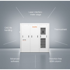
VECTOR is an automated SEM system that consolidates three functions necessary for the evaluation of nano devices—dimensional measurement (CD-SEM), defect inspection, and review—into a single platform. With the incorporation of ultra-high precision thermal shields and laser interferometer stages that remain stable even in harsh environments, it maintains excellent positioning accuracy on the nano order in laboratory conditions with vibrations and temperature changes, automatically acquiring thousands of images and data points. It features defect inspection and recipe-based automated workflows, allowing for stable evaluations regardless of the user's experience level. 1. Metrology - Fully automated measurement and observation of full wafer size - Effective for observing patterning trends on wafers and evaluating tolerances 2. SEM Review - KLARF navigation across the entire wafer - Re-detection and observation of high-contrast defects 3. SEM Inspection - Inspection of critical areas through defect detection - AI-based automatic defect detection and classification
Inquire About This Product
basic information
- Fully automatic observation and measurement - AI-based automatic defect detection and classification - Defect review function through CPI inspection and KLARF navigation (function) - Compatible with Raith's EB lithography equipment, EBPG series. Instant linking of drawing parameters (patterns, dose amounts, etc.) with CD-SEM measurement data. - Optimal for prototyping due to high-speed imaging (approximately 3,000 images captured in 5 hours)
Price range
Delivery Time
Applications/Examples of results
- Fully automated measurement, defect inspection, and observation of full wafers - CD mapping (process window) for DOE conditions - Comparison of gap width in CAD design and CD measurement results - Evaluation of CDU (Critical Dimension Uniformity) and LER (Line Edge Roughness) - Automatic SEM imaging and defect detection/classification
Detailed information
-
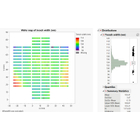
Observation of CD distribution and trends at the full wafer level.
-
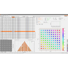
Visualization of measurement and defect inspection results
Line up(1)
| Model number | overview |
|---|---|
| VECTOR |
catalog(1)
Download All Catalogs
Company information

Hakuto Co., Ltd. is a trading company specializing in electronics and providing technical services as a technology trading company and a manufacturer of chemical industrial products, creating a rich future where people and technology coexist by identifying individual needs. Our company was established in November 1953 as a trading company engaged in the import and sale of quartz crystals. The name "Hakuto" is derived from the first character of "Brazil," the origin of quartz, and "Tokyo," representing the east. This name embodies our strong desire to grow as an international trading company that connects not only Brazil and Tokyo but also the wider world. 【Manufacturers/Products Listed on Ipros】 Asahi Kasei / Sensors, Hall elements, ICs Crystal IS / UVC (Deep Ultraviolet) LEDs IMPINJ / RAIN RFID devices, systems, software

