
High-speed signal processing with 16 parallel NCOs
FPGA implementation in JESD204B, suitable high-speed sampling processing methods for RFSOC.

This is an NCO that increases the sampling frequency by 16 times by simultaneously outputting 16 points of sin/cos in one clock cycle.
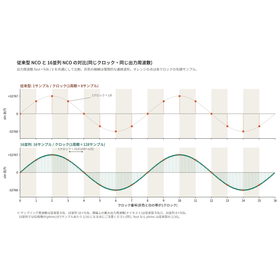
1. What is NCO NCO (Numerical Controlled Oscillator) is a mechanism that generates sin/cos waves using digital circuits. The output frequency is determined by the increment amount (phiinc). 2. Challenges of Conventional Type The conventional type can only output one sample per clock. The maximum output frequency is half of the clock frequency (fclk / 2). To create high-frequency signals, the only option is to increase the clock speed. 3. Concept of 16 Parallel In one clock, 16 samples (x00 to x15) are output simultaneously. The samples are arranged in chronological order, and the sampling frequency is 16 times the clock frequency (16 × fclk). 4. How to Create Phase The phase of lane k is "reference phase + k × phiinc." The reference phase is created by adding phiinc to the phase of the last lane (x15) from the previous clock. Therefore, the waveform does not break at the clock boundary. 5. Circuit Configuration Input register → Constant multiplication (×0 to ×15) → Addition → Phase register → DDS IP ×16 in that order. The phase loop generates the reference phase for the next clock.
Inquire About This Product
basic information
16-Sample Parallel Output NCO (Numerically Controlled Oscillator) - Outputs sin/cos for 16 samples, each advancing by phiinc per clock - Effective sample rate is 8 times the clock; x00 is the oldest sample in time, x07 is the newest sample - The phase of each sample is as follows: phase_k(n) = base(n) + k·phiinc (mod 2^32), base(n+1) = phase_7(n) + phiinc - Uses 16 instances of Xilinx's DDS Compiler v6.0 for sin/cos generation
Price range
Delivery Time
Applications/Examples of results
High-speed signal processing using JESD204B IP for FPGA implementations by AMD (XILINX), INTEL, etc. High-speed I/F circuits for ADCs and DACs of RFSOC like XILINX.
Detailed information
-
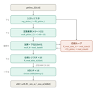
16 Parallel Version Flowchart Input: The input is only phiinc_i. Number of lanes: Multiplication is ×0 to ×15, with 16 phase registers and 16 DDS IPs each, outputting 16 samples of SINCOS data from x00 to x15 in 1 CLK. Phase loop: The data to be held is mod_data15 from the final lane. The reference phase is generated from mod_data00 of lane 0. Latency: As indicated by T+1 to T+8, it takes 8 clocks from phiinc_i to output.
-
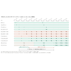
Timing chart diagram With phiinc set to a constant value φ, the changes of the main signals from phiinc_i to the outputs x00/x15 are arranged. Input side: phiinc_i, reg_phiinc_i, ff2_phiinc_i, mult_phiinc_i15 (15φ) Phase loop (red series): mod_data00, mod_data15, ff_mod_data_in Phase register and output: ff_mod_data_o00/o15, sin/cos of x00/x15 (S(p) is the sin/cos for the upper 16 bits of phase p) The lower arrows indicate that from T+1 to T+3 to the phase register, the DDS IP takes 5 clocks, and the first valid output occurs at T+8.
Company information

We provide comprehensive support from idea and specification proposals to development and manufacturing. We consistently design without interruption from analog front-end to high-speed digital, FPGA logic, and edge AI, building high-bandwidth, low-latency, and highly reliable electronic systems for IoT/communication, industrial equipment, broadcasting, measurement, and next-generation mobility. By integrating high-frequency design, signal processing, and real-time control, we ensure that the required specifications are met while proposing improvements where necessary, achieving a high level of completion in implementation.


![We respond to customization of biological signal processing and analysis [in-house development].](https://image.mono.ipros.com/public/product/image/6c8/2001220326/IPROS70780575190375287078.png?w=280&h=280)

