Integration of SECS/GEM communication and OHT handling enables unmanned 24-hour monitoring in fully automated factories!
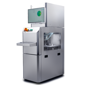
The "SIRD SiC 200" is a system that recognizes and visualizes stress fields, defects, and buried structures within semiconductor wafers quickly, non-contact, and non-destructively. When there is stress within the material, it utilizes the photoelastic effect, where the polarization state of the probe laser changes. Various defects have unique stress fields, and this product optically visualizes them in a non-contact and non-destructive manner, detecting deviations early in the process chain. 【Features】 ■ Quantitative measurement of stress: Quantitative stress measurement at the wafer level ■ Wide doping range: Supports doping levels up to a resistivity of 5.1 mΩ·cm ■ Fully automated: Recipe-based measurement and analysis, compatible with SECS/GEM and OHT ■ Diverse semiconductor materials: Si, SiC, GaN, GaAs, InP, AlN, etc. *For more details, please download the PDF (English version) or feel free to contact us.
Inquire About This Product
basic information
For more details, please download the PDF (English version) or feel free to contact us.
Price range
Delivery Time
Applications/Examples of results
For more details, please download the PDF (English version) or feel free to contact us.
catalog(1)
Download All Catalogs
Company information

PVA Japan LLC provides advanced systems and measurement solutions that drive progress in major industrial sectors around the world. From semiconductors to aerospace technology, we develop and manufacture innovative systems for the production, refinement, and inspection of advanced materials across a wide range of industries. We also offer advanced solutions for acoustic, chemical, and optical inspection and analysis of materials and components. Our portfolio of products and technologies enables efficient, reliable, and scalable high-quality production.