Future Trends of the Global Photolithography Equipment Industry 2026: Growth Path from 40,440 Million USD to 68,122 Million USD
What is a photolithography device? A photolithography device is a manufacturing equipment that forms fine circuit and structural patterns on silicon wafers or substrates coated with photosensitive materials using light or electron beams. Against the backdrop of semiconductor miniaturization, the production of advanced chips for AI, and the advancement of cutting-edge packaging, the photolithography device market is expected to expand. Global market size of photolithography devices According to the latest research report published by Global Reports, "Global Market Size, Share, Company Rankings, Sales, and Demand Trend Forecast for Photolithography Devices (2026-2032)," the global market is expected to expand from 31.53 billion USD in 2025 to 40.44 billion USD in 2026, with an average annual growth rate (CAGR) of 9.1% from 2026 to 2032, and is projected to reach 68.12 billion USD by 2032.
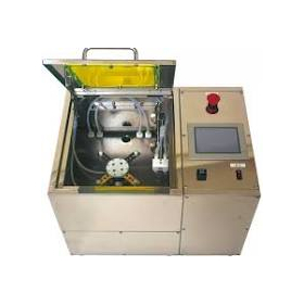
Inquire About This Product
basic information
Technical Classification and Applications of Photolithography Equipment Photolithography equipment is classified into various types, including IC exposure equipment for front-end processes, exposure equipment for advanced packaging, electron beam lithography (EBL) systems, laser direct write (DLW) systems, digital maskless exposure systems, photomask writing systems, laser direct imaging (LDI) systems, focused ion beam (FIB) systems, and nanoimprint lithography (NIL) systems. Exposure technologies include EUV, ArF, KrF, i-line, ultraviolet lasers, digital light modulation, and electron beams. Applications extend to wafers, photomasks, printed circuit boards (PCBs), IC substrates, and displays, with demand areas expanding from semiconductor front-end processes to high-density packaging, optical devices, and MEMS.
Price range
Delivery Time
Applications/Examples of results
Competitive Structure of the Photolithography Equipment Market In the EUV and DUV exposure equipment for advanced semiconductors, ASML holds a leading position, while Nikon and Canon also develop their businesses in mature processes, special applications, and advanced packaging. Canon's nanoimprint technology is gaining attention as a patterning method different from optical projection. In mask drawing, companies such as IMS Nanofabrication, NuFlare Technology, Mycronic, and in electron beam drawing, JEOL, RAITH, Vistec, and Crestec are mentioned as related companies. In the fields of advanced packaging and direct drawing, Onto Innovation, EV Group, SUSS, SCREEN, and Ushio are also important supply companies.
Company information

Global Reports integrates industrial information from around the world and provides highly accurate market intelligence to support corporate decision-making. We deliver in-depth analyses based on numerical data and facts, including market size, share, industry structure, price trends, growth forecasts, rankings of major companies, and competitive trends, with clear information categorized by country, region, and application. Leveraging a rich database that has supported the business growth of over 65,000 companies and an international research network, we accompany our clients in their global expansion and continuous growth.