

Large area sputtering is possible! Film deposition can be achieved even without cooling.


High-performance, cost-effective RF/DC magnetron sputtering device for research and development.

A film deposition platform for semiconductor wafers and advanced packaging capable of various film deposition treatments.


The electron backscatter diffraction method (EBSD) is useful for evaluating the performance of aluminum sputter films and selecting substrate materials.


This is a research and development sputtering device suitable for various film deposition applications, featuring high-level specifications and a wide range of options.
High-performance, cost-effective RF/DC magnetron sputtering system for research and development.

Higher productivity for PLP! More process possibilities. Optimized for advanced packaging.

Flexibility, compact design, and low investment costs! An ideal choice for small-scale production.


Optimal solution for high-rate reactive film deposition production equipment.

Under the management philosophy of 'pursuing customer satisfaction and technical expertise to the utmost and contributing to society,' we develop our business.

An ultra-high temperature substrate heating stage that allows for substrate elevation, rotation, and RF/DC substrate bias all in one device! 'All-In-One' component.

Storage-compatible glove box PVD flexible thin film experimental device, featuring a tall chamber with a height of 570mm, contributes to improved uniformity during deposition.

Due to its modular embedded design, it is possible to flexibly assemble dedicated machines according to the required film formation methods. A compact thin-film experimental device that can accommodate various research applications.

Compact and space-saving! Ideal for research and development, flexible configuration for purposes such as deposition, sputtering, and annealing.


■Advantages ・Custom-made to meet your requirements ・Uniform gas diffusion ・Standard connector elements

It is possible to operate and monitor voltage and current settings.


A research membrane environment that aims to eliminate oxygen and moisture! Supports multilayer membranes, compound membranes, and reactive membranes!


Ion beam sputtering equipment for research and development as well as small-scale production!

The "FHR.Star.600-EOSS" is a high-performance magnetron sputtering device developed for precise optical filter film deposition.


Effective area of a 25mm side triangle! It forms a composition distribution of hundreds of conditions on a single substrate.


We propose value-added products with antibacterial and deodorizing properties through vacuum sputtering processing on fibers and films.


Ideal for experiments, research, evaluation, and prototype production! Achieving high-speed, high-precision, low-damage vacuum deposition on flat substrates such as glass and metal!


There are five expansion slots, allowing for additional installation of sputter chambers, deposition devices, glove boxes, etc.


Inverted sputtering is also possible! Equipped with a 500W high-frequency power supply, it can deposit metals, oxides, insulators, and more.


Maximum 200mm diameter substrate! Double ring magnetron (Fraunhofer FEP)


Using sputtering technology in a medium vacuum environment, we have developed the world's first plating seed layer formation technology through direct copper deposition! Achieving productivity beyond conventional levels!


Equipped with three sources of cathodes in a compact tabletop size. It is also possible to produce insulating thin films, oxide, and nitride thin films.


Various high-precision pressure sensors necessary for flow control in semiconductor manufacturing equipment. Customization of modules is also possible.

Would you like to introduce the PACE series for pressure calibration testing on the manufacturing line? It is also possible to reduce production costs!

Equipped with a simple yet φ3-inch target magnetron cathode and a wide-range turbo molecular pump with a capacity of 200 L/s.


Support from research and development to mass production!

A lineup with over 20 years of proven history. Customized processes and hardware for high-end niche processes from R&D to mass production.


Surface treatment device for sputtering ion gun


Introducing a case study of a sputtering device capable of automatically creating multilayer films!


We have achievements such as 'sputtering equipment with GB for organic EL' and 'IBS equipment for research and development'!


High-precision alignment (within 1μm of the target) is now possible in all directions of X-Y-Z-θx-θy-θz.


Resistance heating evaporation source for the multi-purpose vacuum deposition device HEX system.

Multipurpose Vacuum Deposition Device HEX System Sample Stage | Fixed, Rotating, Rotating Heating, Rotating Water Cooling


This device can clean adhesive rolls during maintenance more quickly and efficiently, addressing a challenge that has troubled customers across various industries!

Supports work widths of 255, 350, 450, 550, 600, and 750 mm!

Ideal for use in clean rooms! It is a fully automatic system for cleaning rolls.
The ULT roll-to-roll web cleaner device stably removes dust even at a converting production line speed of 300m/min.


Development of new thin films using simultaneous three-source sputtering! Customizable according to experimental content and budget.


Vacuum components compatible with high vacuum and ultra-high vacuum.

Product Variety Vacuum Components - Adapter Series

Sapphire vacuum viewport welded using patented dissimilar material welding technology.

Due to its modular embedded design, it is possible to flexibly assemble dedicated equipment according to the required film formation method. A compact thin-film experimental device that can accommodate various research applications.

Compact and space-saving! Ideal for research and development. Flexible configuration for purposes such as deposition, sputtering, and annealing.

A semi-custom-made thin film experimental device that can be assembled with the desired configuration for processes such as evaporation, sputtering, electron beam (EB) deposition, and annealing.

Sputter Cathode and Co-evaporation Source Mixed Thin Film Experimental Device: Metal deposition, organic deposition, and sputter cathode installed in a compact frame.

High-performance multi-sputtering device 6-element multi-sputter (for Φ4 inch) 4-element multi-sputter (for Φ6, 8 inch)

Introduction of various experimental devices for research and development in semiconductors, electronic devices, fuel cells, displays, and thin film experiments.

High-efficiency magnetron sputtering cathode compatible with RF, DC, and pulse DC for depositing metals and insulators without impurities. It also excels in maintainability.

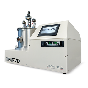
Storage-compatible glove box PVD flexible thin film experimental device, featuring a tall chamber with a height of 570mm, contributes to improved uniformity during deposition.

Composite thin film experimental device nanoPVD-ST15A capable of mixed installation of vacuum deposition (metal and organic deposition sources) and sputtering cathodes.

High-performance multi-sputtering device 6-element multi-sputter (for Φ4 inch) 4-element multi-sputter (for Φ6, 8 inch)

Due to its modular embedded design, it is possible to flexibly assemble dedicated equipment according to the required film deposition method. A compact thin-film experimental device that can accommodate various research applications.

A semi-custom-made thin film experimental device that can be assembled with the desired configuration for processes such as sputtering, EB (electron beam), and annealing.

Flexible configuration available upon request for methods such as deposition, sputtering, and EB. Adopts a tall chamber with a height of 570mm, contributing to improved uniformity during deposition.

Compact and space-saving! Ideal for research and development. Flexible configuration for purposes such as deposition, sputtering, and annealing.

A compact multi-thin film device that incorporates sputtering, deposition, electron beam (EB), and annealing thin film modules in a 60-liter volume chamber, suitable for various applications.

Compact multi-film device that incorporates sputtering, deposition, EB, and annealing thin film modules in a 60L volume chamber, suitable for various applications.

Two thin-film experimental devices are connected with a load-lock mechanism. Different film deposition devices (sputtering, evaporation, etc.) are seamlessly connected with the load-lock.

Two thin film experimental devices are connected with a load lock mechanism. Different film deposition devices (sputtering, evaporation, etc.) are seamlessly connected with the load lock.


This processing requires a significant amount of positioning. We maintain a guarantee of ±0.05.


Meeting the high cleanliness standards required in the semiconductor and medical device fields. We carry out everything from precision cleaning to packaging and assembly in a consistent clean environment.


Shortest half-day estimate / We have accepted the production of equipment parts made of aluminum material.

Shortest half-day estimate / From metal parts to resin products, we introduce components related to semiconductor manufacturing equipment based on our track record!

Polycrystalline silicon is used as a raw material for the semiconductor industry and the solar cell industry (PV). Material: Nickel alloy Process: Filter


You are using SiC/Si composite materials as the target material.

Coating equipment for manufacturing functional films for Flexible Displays.


A method of production that mounts a substrate in a single chamber.


The installation direction can be freely set! Achieving maintenance-free operation with a long lifespan of 30 million rotations!

Custom production is possible according to application from single item prototypes! Lineup includes "EB Gun" and "K Cell"!

The substrate dimensions can accommodate up to 3 pieces with a maximum size of 3 inches! It is equipped with a heating mechanism and a reverse sputtering mechanism!

We will introduce energy semiconductor device research and development systems compatible with φ4-inch substrates!


A film formation technology with excellent reproducibility that utilizes high energy to forge the material itself!

We will give you a free copy of "Thin Film Q&A," which summarizes the differences and characteristics of various coating methods, coating examples, and frequently asked questions!


Compact design yet maintains performance! A sputtering device capable of substrate heating at high temperatures.

It is an introduction device that transmits linear motion from the atmospheric side to samples and equipment in a vacuum.


Experimental device equipped with an ion source, applicable for ultra-thin film multilayer deposition in precision optics.

It is an ion beam sputtering (IBS) device that uses an RF ion source and is equipped with a single stage or planetary stage.


Packaging and packing machines, as well as vacuum pumps! We offer a full range of equipment from the main units to components in various fields.


We offer assembly services mainly related to the installation, assembly, modification, and maintenance of semiconductor manufacturing equipment.


Reduce initial implementation costs and enable high performance through expansion! Upgrade according to the research stage.

Easy discharge operation! Compact design with automatic matching for RF power supply.


Leave the manufacturing of semiconductor sputtering targets to us.


Rich experience in processing various materials and substrates! Substrate × thin film = optical adjustment, conductivity, antibacterial/antiviral.

Rich experience in processing various materials and substrates! Substrate × thin film = optical adjustment, conductivity, antibacterial/antiviral.

Various antibacterial/antiviral treatments, anti-mold, etc.! Sputtering processing on fibers and films.

Rich experience in processing various materials and substrates! Effective sputtering technology for mold prevention as well.

Suppress the growth of bacteria/viruses with metals/alloys! Sputtering processing on fibers is possible.