
List of Semiconductor Manufacturing Equipment products
- classification:Semiconductor Manufacturing Equipment
136~150 item / All 5251 items


It won't break even after 1 million repetitions! A mat switch with reliable operation, high durability, and low price. Suitable for options in machine tools as well. Please consult us about delivery t...
- Sensors


We can accommodate high resistance over 10,000 ohms, with diameters ranging from approximately 30 mm to 8 inches, and we also offer thinning and chip processing arrangements!
- Other semiconductors
- Processing Contract
- Wafer


6 to 8 inch ultra-high temperature wafer annealing equipment, a high-performance machine that widely supports various purposes from research and development to small-scale production.
- Annealing furnace
- Heating device
- Electric furnace

4-Yen Multi-Sputtering Device 【MiniLab-S060】
4 cathodes with Φ2 inch configuration Simultaneous film deposition: 3-component simultaneous deposition (RF 500W or DC 850W) + HiPIMS (PulseDC 5KW) x 1 Power distribution and configuration settings for 4 cathodes can be freely changed via the HMI screen using the plasma relay switch 3 MFC systems (Ar, O2, N2) for reactive sputtering RIE etching stage RF 300W (main chamber) + <30W soft etching (LL chamber) Substrate heating: Max 500℃, 800℃, or 1000℃ (C/C or SiC coating) Substrate rotation and vertical movement (automatically controlled by stepping motor) APC automatic control: Upstream (MFC flow adjustment) or downstream (automatic valve opening adjustment on the exhaust side) Dimensions: 1,120(W) x 800(D) ● Mixed specifications for resistance heating deposition, organic material deposition, EB deposition, PECVD, etc. are also possible.

6 to 8 inch ultra-high temperature wafer annealing equipment, a high-performance machine that widely accommodates various purposes from research and development to small-scale production.
- Annealing furnace

The catalog for the MiniLab Flexible Thin Film Experimental Device has been renewed!
We have completely renewed the catalog for the MiniLab series thin film experimental equipment. 【Features of the MiniLab Series】 ◉ Supports sputtering, evaporation (resistive heating, organic, EB), annealing, plasma etching, etc. ◉ Modular design allows for flexible combinations of components (source hybrid types and multi-chamber configurations are possible) ◉ Compact, space-saving design (width 1,200 x depth 560 mm) ◉ Excellent operability: intuitive interface allows for centralized management of all operations via a touch panel without dispersion. We are confident that this will be of great assistance in research and development settings. Please consider it.
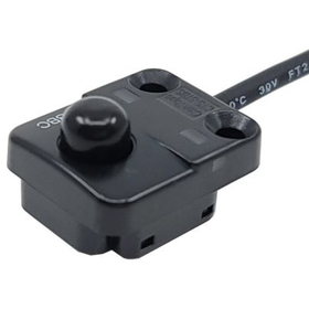

Stable detection unaffected by light noise is possible with contact sensors! Designed for over 10 million high durability cycles.
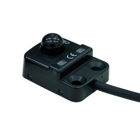
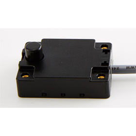
- Other semiconductor manufacturing equipment
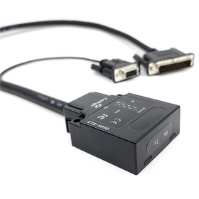
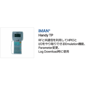
World's first! Wireless E84 sensor
- Other semiconductor manufacturing equipment


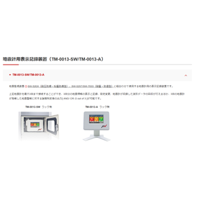
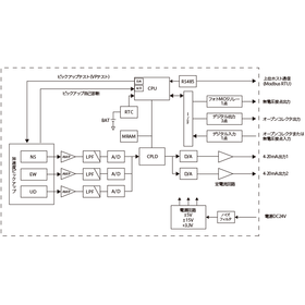
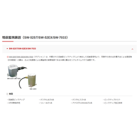
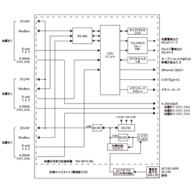
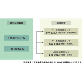
Up to 3 earthquake monitoring devices can be connected.
- Other machine tools
- Semiconductor inspection/test equipment
- Metal bearings


We are a problem-solving company that realizes "visualization" of energy conservation and measurement!
- Other measurement, recording and measuring instruments
- Sensors
- Tester


Achieving high-quality polishing that preserves the edge through automation.
- Wafer processing/polishing equipment

We will exhibit at the SURTECH 2025 trade show.
We will be exhibiting at SURTECH 2025 – Surface Technology Exhibition – which will be held at Tokyo Big Sight from January 29, 2025 (Wednesday). We will introduce the "DLyte," a dry electrochemical polishing machine that uses resin media for ion exchange to grind and polish metals. Exhibition: SURTECH 2025 Location: Tokyo Big Sight, East Hall 3 Organizer: JTB Communication Design, Inc. (Rapid News Publications Ltd.) Date: January 29 (Wednesday) to January 31 (Saturday), 2025 Time: 10:00 AM to 5:00 PM Booth Number: 3X-11 *For inquiries and to download the catalog, please visit here. You can find more detailed information on our website. Request for materials: https://www.nttdata-xam.com/document/ Inquiries: https://www.nttdata-xam.com/contact/

Achieving high-quality polishing that preserves edges through mechanization.
- Wafer processing/polishing equipment
We will exhibit at the SURTECH 2025 trade show.
We will be exhibiting at SURTECH 2025 – Surface Technology Exhibition – which will be held at Tokyo Big Sight from January 29, 2025 (Wednesday). We will introduce the "DLyte," a dry electrochemical polishing machine that uses resin media for ion exchange to grind and polish metals. Exhibition: SURTECH 2025 Location: Tokyo Big Sight, East Hall 3 Organizer: JTB Communication Design, Inc. (Rapid News Publications Ltd.) Date: January 29 (Wednesday) to January 31 (Saturday), 2025 Time: 10:00 AM to 5:00 PM Booth Number: 3X-11 *For inquiries and to download the catalog, please visit here. You can find more detailed information on our website. Request for materials: https://www.nttdata-xam.com/document/ Inquiries: https://www.nttdata-xam.com/contact/

Achieving high-quality polishing that retains the edge through mechanization.
- Wafer processing/polishing equipment
We will exhibit at the SURTECH 2025 trade show.
We will be exhibiting at SURTECH 2025 – Surface Technology Exhibition – which will be held at Tokyo Big Sight from January 29, 2025 (Wednesday). We will introduce the "DLyte," a dry electrochemical polishing machine that uses resin media for ion exchange to grind and polish metals. Exhibition: SURTECH 2025 Location: Tokyo Big Sight, East Hall 3 Organizer: JTB Communication Design, Inc. (Rapid News Publications Ltd.) Date: January 29 (Wednesday) to January 31 (Saturday), 2025 Time: 10:00 AM to 5:00 PM Booth Number: 3X-11 *For inquiries and to download the catalog, please visit here. You can find more detailed information on our website. Request for materials: https://www.nttdata-xam.com/document/ Inquiries: https://www.nttdata-xam.com/contact/

Achieving high-quality polishing that preserves edges through mechanization.
- Wafer processing/polishing equipment
We will exhibit at the SURTECH 2025 trade show.
We will be exhibiting at SURTECH 2025 – Surface Technology Exhibition – which will be held at Tokyo Big Sight from January 29, 2025 (Wednesday). We will introduce the "DLyte," a dry electrochemical polishing machine that uses resin media for ion exchange to grind and polish metals. Exhibition: SURTECH 2025 Location: Tokyo Big Sight, East Hall 3 Organizer: JTB Communication Design, Inc. (Rapid News Publications Ltd.) Date: January 29 (Wednesday) to January 31 (Saturday), 2025 Time: 10:00 AM to 5:00 PM Booth Number: 3X-11 *For inquiries and to download the catalog, please visit here. You can find more detailed information on our website. Request for materials: https://www.nttdata-xam.com/document/ Inquiries: https://www.nttdata-xam.com/contact/

Achieving high-quality polishing that preserves the edge through mechanization.
- Wafer processing/polishing equipment
We will exhibit at the SURTECH 2025 trade show.
We will be exhibiting at SURTECH 2025 – Surface Technology Exhibition – which will be held at Tokyo Big Sight from January 29, 2025 (Wednesday). We will introduce the "DLyte," a dry electrochemical polishing machine that uses resin media for ion exchange to grind and polish metals. Exhibition: SURTECH 2025 Location: Tokyo Big Sight, East Hall 3 Organizer: JTB Communication Design, Inc. (Rapid News Publications Ltd.) Date: January 29 (Wednesday) to January 31 (Saturday), 2025 Time: 10:00 AM to 5:00 PM Booth Number: 3X-11 *For inquiries and to download the catalog, please visit here. You can find more detailed information on our website. Request for materials: https://www.nttdata-xam.com/document/ Inquiries: https://www.nttdata-xam.com/contact/
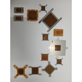

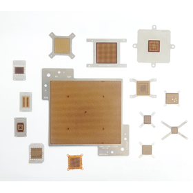
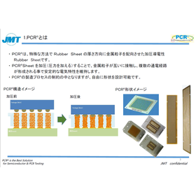
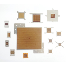
A sheet socket that enables stable inspection in semiconductor back-end process inspection! What is "PCR" that allows for high-speed and high-density measurements? Technical materials on operating pri...
- Other electronic parts
- socket
- Semiconductor inspection/test equipment
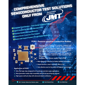
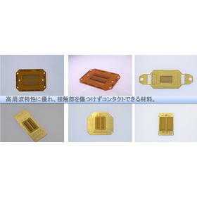
Test solution that does not damage solder balls or measurement substrates with soft contact!
- Semiconductor inspection/test equipment
- Printed Circuit Board

Maximum operating temperature 2000℃ Semi-automatic control Ultra-high temperature experimental furnace (carbon furnace, tungsten metal furnace) Compact and space-saving experimental furnace
- Heating device
- Annealing furnace
- Electric furnace

VOXIA compact X-ray CT imaging device
Compact design with a space-saving layout that can be installed anywhere. Despite its compact body, it generates high-resolution data through advanced calculation software. * X-ray tube voltage: 20-90kV, or 40-maximum 130kV * Focus diameter: 7μm (5μm@4W) * Detector pixel: 89μm, approximately 3.2 million pixels! * Sample size: Φ120mm ◉ Vcap (Control Software): A custom-made imaging stage tailored to the subject and purpose. A series of tasks from shooting to image output can be performed with just a click. High-speed continuous shooting in as fast as 20 seconds, with processing from shooting start to image reconstruction taking about 30 seconds. ◉ VCT (Reconstruction Software): Customizable automatic measurement and analysis software specialized for the specified subject. High-speed reconstruction of shooting data with 992 x 992 pixel images and 600 projections in just 3.8 seconds! ◉ MolcerPlus (3D Display Analysis): Custom software that enables measurement conditions that were difficult with conventional software. Software for displaying, processing, and measuring the imaged object. ● High safety, ● Compatible with a wide variety of samples, ● Intuitive HMI, easy operation.

Maximum operating temperature 2000℃ Semi-automatic control Ultra-high temperature experimental furnace (carbon furnace, tungsten metal furnace) Compact and space-saving experimental furnace
- Heating device
- Annealing furnace
- Electric furnace
4-Yen Multi-Sputtering Device 【MiniLab-S060】
4 cathodes with Φ2 inch configuration Simultaneous film deposition: 3-component simultaneous deposition (RF 500W or DC 850W) + HiPIMS (PulseDC 5KW) x 1 Power distribution and configuration settings for 4 cathodes can be freely changed via the HMI screen using the plasma relay switch 3 MFC systems (Ar, O2, N2) for reactive sputtering RIE etching stage RF 300W (main chamber) + <30W soft etching (LL chamber) Substrate heating: Max 500℃, 800℃, or 1000℃ (C/C or SiC coating) Substrate rotation and vertical movement (automatically controlled by stepping motor) APC automatic control: Upstream (MFC flow adjustment) or downstream (automatic valve opening adjustment on the exhaust side) Dimensions: 1,120(W) x 800(D) ● Mixed specifications for resistance heating deposition, organic material deposition, EB deposition, PECVD, etc. are also possible.