
List of Semiconductor Manufacturing Equipment products
- classification:Semiconductor Manufacturing Equipment
2086~2100 item / All 5179 items


Reduce the workload from handling heavy objects! Here are five case studies that solved customer challenges! We are also accepting free consultations and tests tailored to your work!

- Other conveying machines


Ideal for micro-machining! Achieves deburring of holes and double-sided machining in one pass, which was difficult with conventional tools!

- Other machine tools

We will be exhibiting at Mecatronics Tech Japan 2021 from October 20 (Wednesday) to October 23 (Saturday)!
Our company will exhibit at "Mechatrotech Japan 2021," which will be held at Portmesse Nagoya from Wednesday, October 20 to Saturday, October 23, 2021. We will introduce our tools, including the 'Bar Off Tool' capable of chamfering and deburring from a diameter of 0.8 mm, and the 'FEM' tool breakage detection device that reliably detects breakage. We look forward to your visit. (Booth number: 2B12)


We provide custom design and manufacturing of semiconductor and electronic component-related equipment from various labor-saving machines.
- Other semiconductor manufacturing equipment


A lineup of lens polishing machines that can accommodate various optical surfaces and interferometers that can measure flat shapes without being affected by the back surface.
- Wafer processing/polishing equipment


Kaneko Chemical Cleaning Agent Product Line
- Annealing furnace


Value Impact Co., Ltd. offers value in "connecting." We provide tube fittings used for vacuum piping and high-pressure gas piping.
- Other semiconductor manufacturing equipment


Highly versatile UV, green, and IR picosecond lasers: The new standard in picosecond micromachining.
- Wafer processing/polishing equipment

High-output UV and femtosecond lasers enable high-quality, high-precision processing of difficult materials at high speed.
- Wafer processing/polishing equipment


We will design the layout of each chamber and pump according to the installation location.
- Etching Equipment


Plasma cleaner with a parallel plate method, optimal for cleaning bonding pads (improving bondability) and surface modification/hydrophilization (molding pretreatment).
- Other semiconductor manufacturing equipment


Surface modification, cleaning, hydrophilicity treatment, and adhesion enhancement with excellent low-temperature charge damage-free performance! Pen-type atmospheric pressure plasma device!
- Other semiconductor manufacturing equipment
- Bonding Equipment
- Circuit board processing machine
![[Domestic] Vacuum Plasma Device (49...](https://image.mono.ipros.com/public/product/image/4ed/2000127084/IPROS91047023304598935134.png?w=280&h=280)
Excellent low-temperature charge damage-free surface modification and cleaning! Affordable vacuum and atmospheric pressure plasma available!
- Etching Equipment


We will give you a free copy of "Thin Film Q&A," which summarizes the differences and characteristics of various coating methods, coating examples, and frequently asked questions!
- Surface treatment contract service
- Sputtering Equipment
- Ceramics

Leave your analysis requests to us! Free download of the "Analysis Equipment List"!
The evaluation of thin films is determined by the purpose for which the thin film is used. For example, if the thin film is used for enhancing mechanical strength, important factors for evaluation include hardness and adhesion. If the film is intended to impart optical properties, values such as reflectivity and transmittance become important. Toho Kaken has three main divisions: the "Ion Plating Division," the "Material Analysis Division," and the "Environmental Analysis Center," which allows us to possess a wide range of analytical equipment. In addition to requests for thin film coating, we can also handle analysis and evaluation. We also accept inquiries for "inspection and analysis only" apart from thin film coating, so please feel free to contact us!


Optimized thermal design for handling delicate organic materials! Suppressing thermal effects on evaporated substances and substrates.
- Evaporation Equipment

Robust and scalable design! High-energy, strongly focused beam.
- Electron beam lithography equipment
![[Business Introduction] Special App...](https://image.mono.ipros.com/public/product/image/c79/2000804205/IPROS25324904358444298624.png?w=280&h=280)
Special order support team! Providing ideal solutions for large-scale production.
- Electron beam lithography equipment
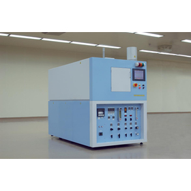

A quartz tube type annealing device commonly used for alloying and reducing resistance of electrode films in compound semiconductors. It is a high-temperature processing type equipped with a rapid coo...
- Annealing furnace
- Heating device