
List of Semiconductors and ICs products
- classification:Semiconductors and ICs
2911~2925 item / All 4817 items


Reduce the workload from handling heavy objects! Here are five case studies that solved customer challenges! We are also accepting free consultations and tests tailored to your work!

- Other conveying machines


Ideal for micro-machining! Achieves deburring of holes and double-sided machining in one pass, which was difficult with conventional tools!

- Other machine tools

We will be exhibiting at Mecatronics Tech Japan 2021 from October 20 (Wednesday) to October 23 (Saturday)!
Our company will exhibit at "Mechatrotech Japan 2021," which will be held at Portmesse Nagoya from Wednesday, October 20 to Saturday, October 23, 2021. We will introduce our tools, including the 'Bar Off Tool' capable of chamfering and deburring from a diameter of 0.8 mm, and the 'FEM' tool breakage detection device that reliably detects breakage. We look forward to your visit. (Booth number: 2B12)


Adopting SiC-MOSFET as the switching element significantly reduces power loss.
- Other semiconductors


The ball diameter is φ5/8" (15.88mm)! Another standard for cleanroom iguchi bearings.
- Other semiconductors

The adoption results that began from the post-processing of LCDs are now being utilized in various processing stages, and the lineup of positioning stages has also increased.
- Other semiconductors
![[Development Case] Data Recording D...](https://image.mono.ipros.com/public/product/image/d47/2000823019/IPROS15181591032565440259.jpeg?w=280&h=280)

A model case that encompasses the overall development, including specifications summary, chassis design, and program design!
- Memory


Multiple light-emitting elements in one package! Customization according to your preferences is possible!


- Transistor

Multi-wavelength emitter
The "Multi-Wavelength Emitter" from Marktech, provided by Rikei, integrates multiple light-emitting elements (2 to 7) into a single package. You can choose light-emitting elements from UV to short-wavelength infrared (SWIR). Additionally, the implementation of light-receiving elements is also possible. By combining Si PD/InGaAs PD, light sensing at multiple wavelengths can be performed in one package. Please feel free to consult us regarding the wavelength range you wish to use. Custom solutions are also available. You can download the product list and specifications from the related catalog below.


Due to the dry process, no water is used, making it environmentally friendly. Achieves increased productivity with zero car floss. Compared to conventional methods, it reduces the footprint.
- Wafer
- LCD display
- Fine Ceramics

Due to the dry process, no water is used, making it environmentally friendly. Achieves increased productivity with zero car flows. Compared to conventional methods, it has a smaller footprint.
- Wafer
- LCD display
- Fine Ceramics


We provide the parts you want with short delivery times and low costs. We have numerous transaction records with major domestic companies. We are also accepting purchase appraisals.
- Other electronic parts
- Other machine elements
- Other semiconductors

A wide variety of package types! Emitters (light-emitting elements) from 1,020 to 1,720 nm.


- Transistor


Even with a 10mm corner, it is possible depending on the processing method! During prototype development, we can process from just one piece.
- Processing Contract
- Circuit board design and manufacturing
- Other semiconductors


A semiconductor package that supports miniaturization and high density through unique cavity structure formation technology.
- Other electronic parts
- Circuit board design and manufacturing
- Other semiconductors
![[Technical Introduction] Semiconduc...](https://image.mono.ipros.com/public/product/image/9b3/2000816074/IPROS48867073461765814843.png?w=280&h=280)

From the design and manufacturing of molds to the assembly of stamping molds, we mass-produce and supply various lead frames with high precision and high quality.
- Other semiconductors
- Other molds

Mass production of high-precision, high-quality lead frames for high-quality semiconductor devices, including deep pressing and bending!
From the design and manufacturing of molds to the assembly of stamping molds, we mass-produce and supply various lead frames with high precision and high quality. There are many types of lead frames used in semiconductor devices. At Rohm Mecatech, we produce lead frames using stamping molds and have numerous achievements in lead frames that require deep pressing/bending. If you could provide us with the desired shape of the frame, we will consider whether we can accommodate it and conduct a technical review, so please feel free to let us know. 【Process for Requesting Lead Frames】 ■ Send the drawings of the lead frame you wish to manufacture ■ After a technical review to determine feasibility, we will submit a quotation ■ Order and manufacture the stamping mold ■ Begin mass production after the stamping mold is completed *For more details, please refer to the PDF materials or feel free to contact us.
![[Technical Introduction] Lead Frame...](https://image.mono.ipros.com/public/product/image/ac1/2000816060/IPROS24277109310485626781.png?w=280&h=280)
The achievements in lead frame support are diverse! We are mass-producing and supplying with high precision and high quality.
- Other semiconductors
- Other molds

[Technical Introduction] Lead Frames for Semiconductor Transistors
The achievements in lead frame support are diverse! We are mass-producing and supplying with high precision and high quality. At Rohm Mecatec, we produce lead frames for transistors using stamping molds. We have established a large-scale production system both in Japan and overseas, allowing us to respond quickly to customer requests with ample capacity. If you could provide us with the desired shape of the frame, we will conduct a technical review to see if we can accommodate your request, so please feel free to reach out. 【Process for Lead Frame Requests】 ■ Send us the drawings of the lead frame you wish to produce. ■ After a technical review to determine feasibility, we will submit a quotation. ■ Place an order for the stamping mold and proceed with production. ■ Once the stamping mold is completed, mass production will begin. *For more details, please refer to the PDF document or feel free to contact us.
![[Technical Introduction] Lead Frame...](https://image.mono.ipros.com/public/product/image/7b3/2000816025/IPROS97449249735013610456.png?w=280&h=280)
Leave the lead frames for tantalum capacitors to us.
- Other semiconductors
- Other molds
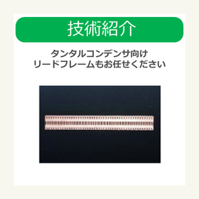
Lead frame experts: Rohm Mecatech offers the best manufacturing solutions for tantalum capacitors.
Please leave the lead frames for tantalum capacitors to us. At Rohm Mecatech, we produce lead frames for tantalum capacitors using stamping molds. We have a large-scale production system both in Japan and overseas, with ample capacity to respond quickly to customer requests at any time. If you could provide us with the desired shape of the frame, we will conduct a technical review to see if we can accommodate it, so please feel free to reach out. [Process for Requesting Lead Frames] ■ Send us the drawings of the lead frame you wish to produce ■ After a technical review to determine feasibility, we will submit a quotation ■ Order and production of the stamping mold ■ Start mass production after the stamping mold is completed *For more details, please refer to the PDF materials or feel free to contact us.
![[Technical Introduction] Please lea...](https://image.mono.ipros.com/public/product/image/2e3/2000816016/IPROS74189470566848952191.png?w=280&h=280)
Large-scale production system! There are various types of lead frames used in semiconductor devices.
- Other semiconductors
- Other molds