
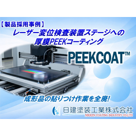
To semiconductor and LCD inspection equipment! Thick-film PEEK coating compatible with large components.
Numerous achievements in the semiconductor and FPD industries. We solve issues related to scratches, distortions, and cost challenges for stages, hands, and tanks. We are also accepting orders for prototype construction of large works ranging from 1 to 2 meters!
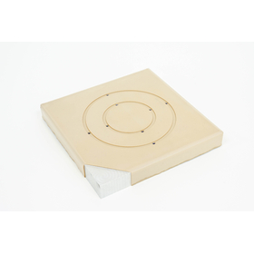
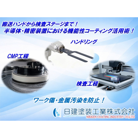
In semiconductor and liquid crystal (FPD) manufacturing and inspection equipment, where high cleanliness and micron-level precision are required, the surface treatment of stages and transport components that come into direct contact with the workpiece significantly affects the reliability of the equipment. Our company offers contract processing solutions for large precision components using high-performance PEEK coating "PEEKCOAT." [Our Strengths and Value Proposition] ■ Large Equipment Available We can perform bulk processing of large stages and long arms sized 1 to 2 meters. ■ "Thick Film + Post-Processing" Technology By baking a PEEK coating film of over 1mm and then finishing it with precision machining, we achieve both stringent dimensional accuracy and smooth surface protection performance. ■ Advanced Distortion Control We possess specialized jig technology that suppresses deformation and shrinkage stress of the substrate due to firing heat of approximately 400°C. [Horizontal Expansion and Abundant Processing Achievements] We have numerous surface treatment achievements for various components in semiconductor and liquid crystal equipment, including inspection stages, transport hands, CMP peripheral components, cleaning and etching tanks, piping, and chambers. Please feel free to consult us for test processing (prototyping) tailored to your challenges.
- Company:日建塗装工業
- Price:Other






![[English Market Research Report] The Global Market for Textile Coatings](https://image.mono.ipros.com/public/product/image/506/2001161419/IPROS12071102988241827780.png?w=280&h=280)

![[English Market Research Report] European Protective Coatings Market](https://image.mono.ipros.com/public/product/image/382/2001182996/IPROS15750403468823253374.png?w=280&h=280)
![[English Market Research Report] Global Market for Construction Coatings](https://image.mono.ipros.com/public/product/image/02c/2001182997/IPROS2909612437471802444.png?w=280&h=280)
![[English Market Research Report] Global Market for Protective Coatings](https://image.mono.ipros.com/public/product/image/692/2001182998/IPROS7947771470917526269.png?w=280&h=280)

![[English Market Research Report] Graphene Coating Market](https://image.mono.ipros.com/public/product/image/80b/2001208174/IPROS16825372862973482934.png?w=280&h=280)


![Maintenance cost reduction coating BARIAS [Powder adhesion suppression] V](https://image.mono.ipros.com/public/product/image/92d/2000515479/IPROS08179213330897013072.jpeg?w=280&h=280)

