We have compiled a list of manufacturers, distributors, product information, reference prices, and rankings for Resist.
ipros is IPROS GMS ・ IPROS One of the largest technical database sites in Japan that collects information on.

Resist Product List and Ranking from 15 Manufacturers, Suppliers and Companies | IPROS GMS

Last Updated: Aggregation Period:Sep 09, 2026~Oct 06, 2026
This ranking is based on the number of page views on our site.

Resist Manufacturer, Suppliers and Company Rankings

Last Updated: Aggregation Period:Sep 09, 2026~Oct 06, 2026
This ranking is based on the number of page views on our site.

  1. ハニー化成 Hyogo//Chemical
  2. プリケン 本社、山形営業所、神奈川営業所、関西営業所、福岡営業所 Saitama//Electronic Components and Semiconductors
  3. TAMURA CORPORATION Tokyo//Industrial Electrical Equipment
  4. 4 ケイ・オール Tokyo//Manufacturing and processing contract
  5. 5 RION Co., Ltd. Tokyo//Testing, Analysis and Measurement

Resist Product ranking

Last Updated: Aggregation Period:Sep 09, 2026~Oct 06, 2026
This ranking is based on the number of page views on our site.

  1. Photosensitive coverlay for flexible circuit boards. TAMURA CORPORATION
  2. What is solder resist that you can't ask about now? ケイ・オール
  3. What is photoresist for LEDs? A collection of basic knowledge. ハニー化成
  4. 4 What is photoresist for LCD displays? A collection of basic knowledge. ハニー化成
  5. 4 What is photoresist for solar cells? A collection of basic knowledge. ハニー化成

Resist Product List

31~45 item / All 45 items

Displayed results

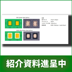
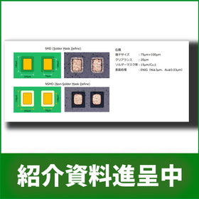
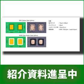
Technical Documentation on Solder Resist Formation for Game Consoles

Presented is a document summarizing the specifications for heat dissipation measures for game consoles!

In the gaming console industry, as performance increases, heat dissipation measures for circuit boards have become crucial. In particular, to handle high thermal density within limited space, the selection of appropriate solder resist is essential. Inappropriate solder resist can hinder heat conduction, potentially leading to decreased product performance or failure. Our materials on solder resist formation technology include specifications such as terminal size, clearance, solder mask thickness, and surface treatment, which are useful for product selection. 【Application Scenarios】 - Circuit board design for high-performance gaming consoles - Selection of circuit boards requiring heat dissipation measures - Design of compact and high-density mounted circuit boards 【Benefits of Implementation】 - Improved heat dissipation through appropriate solder resist selection - Enhanced product reliability - Reduction in design workload

Added to bookmarks

Bookmarks list

Bookmark has been removed

Bookmarks list

You can't add any more bookmarks

By registering as a member, you can increase the number of bookmarks you can save and organize them with labels.

Free membership registration

What is photoresist for MEMS? A collection of basic knowledge.

Fundamental knowledge of photoresist essential for microstructure processing in MEMS.

In the field of MEMS, high-precision pattern formation is required for microstructure processing. Particularly, understanding the properties of photoresists and selecting the appropriate ones are crucial for accurately creating fine circuits and structures. The use of inappropriate photoresists or errors in the process can potentially affect the reproducibility of microstructures and the performance of devices. This page explains the basic knowledge of photoresists, their types, process images, coating methods, and the features of our electrostatic resist, contributing to solving challenges in microstructure processing in the MEMS field. 【Application Scenarios】 - Prototyping and development of MEMS devices - Formation of fine circuit patterns - Product development requiring high-precision structural processing 【Benefits of Introduction】 - Acquisition of basic knowledge about photoresists - Promotion of understanding of negative and positive types - Visualization of process images - Understanding of the coating methods for liquid photoresists - Grasping the characteristics of electrostatic resist

  • Printed Circuit Board
  • Other electronic parts
  • Technical and Reference Books
  • Resist

Added to bookmarks

Bookmarks list

Bookmark has been removed

Bookmarks list

You can't add any more bookmarks

By registering as a member, you can increase the number of bookmarks you can save and organize them with labels.

Free membership registration

What is photoresist for microelectronics? A collection of basic knowledge.

Explaining the basic knowledge of photoresist essential for high-density packaging.

In the microelectronics industry, particularly in high-density packaging, there is a demand for technologies that can accurately form fine circuit patterns. Photoresist plays a very important role in this microfabrication process as a photosensitive material that enables pattern formation through exposure. Inappropriate selection or use of photoresist can lead to a decrease in circuit accuracy and the occurrence of defects. Our company has been responding to our customers' advanced needs through the manufacturing and sales of electrodeposited resist. In light of the importance of providing information on the basic knowledge of photoresist, we have created this basic knowledge page. It explains the fundamental mechanisms of photoresist, the differences between negative and positive types, specific process images, and the application methods for liquid photoresist. Additionally, we also introduce the features of our electrodeposited resist, so please feel free to download the catalog. 【Usage Scenarios】 - Fine circuit patterning in semiconductor manufacturing - Manufacturing processes for high-density packaging substrates - Precision processing of electronic components 【Benefits of Implementation】 - Improved accuracy of circuit patterns - Stabilization of manufacturing processes - Enhanced product reliability

  • Printed Circuit Board
  • Other electronic parts
  • Technical and Reference Books
  • Resist

Added to bookmarks

Bookmarks list

Bookmark has been removed

Bookmarks list

You can't add any more bookmarks

By registering as a member, you can increase the number of bookmarks you can save and organize them with labels.

Free membership registration

What is photoresist for solar cells? A collection of basic knowledge.

Basic knowledge of photoresist essential for electrode formation in solar cells.

In the manufacturing process of solar cells, high-precision electrode pattern formation is required. In particular, the miniaturization and uniformity of electrodes, which are directly related to light energy conversion efficiency, are crucial factors that influence product performance. Improper pattern formation can lead to a decrease in power generation efficiency and a reduction in product lifespan. Photoresist is an essential material for achieving this precise pattern formation. Our company supports the resolution of your technical challenges through the manufacture and sale of electrodeposition resist. 【Application Scenarios】 - Formation of electrode patterns for solar cells - Manufacturing of electronic components requiring fine processing 【Benefits of Implementation】 - Formation of high-precision electrode patterns - Contribution to improving the power generation efficiency of solar cells - Enhancement of product reliability

  • Printed Circuit Board
  • Other electronic parts
  • Technical and Reference Books
  • Resist

Added to bookmarks

Bookmarks list

Bookmark has been removed

Bookmarks list

You can't add any more bookmarks

By registering as a member, you can increase the number of bookmarks you can save and organize them with labels.

Free membership registration

What is Photoresist for the Printing Industry? A Collection of Basic Knowledge

I will explain the basic knowledge of the printing process in an easy-to-understand manner.

In the printing industry’s plate-making process, precise pattern formation is required. Particularly, to accurately reproduce fine circuits and designs, it is important to understand and properly handle the characteristics of photoresist. If the selection and usage of photoresist are inadequate, the accuracy of plate-making may decrease, potentially affecting the quality of the final printed materials. This page comprehensively explains the basic knowledge of photoresist, the differences between negative and positive types, process images, coating methods, and the features of our electrodeposited resist, helping to deepen your understanding in your plate-making operations. 【Usage Scenarios】 - Acquisition of basic knowledge about photoresist in the plate-making process - Understanding of negative and positive photoresists - Confirmation of coating methods for liquid photoresist - Grasping the features of electrodeposited resist 【Effects of Implementation】 - Improvement in the accuracy of the plate-making process - Resolution of questions regarding photoresist - Support for appropriate photoresist selection - Consideration of the use of electrodeposited resist

  • Printed Circuit Board
  • Other electronic parts
  • Technical and Reference Books
  • Resist

Added to bookmarks

Bookmarks list

Bookmark has been removed

Bookmarks list

You can't add any more bookmarks

By registering as a member, you can increase the number of bookmarks you can save and organize them with labels.

Free membership registration

What is photoresist for biochips? A collection of basic knowledge.

Basic knowledge of photoresists useful for microchannel formation.

In the field of biochips and the formation of microfluidic channels, precise patterning is required. Particularly, the appropriate selection and application of photosensitive materials are crucial for accurately creating fine structures. Inappropriate materials or processes can lead to variations in channel dimensions and functional failures. This page explains the fundamental knowledge of photoresists, which are essential for semiconductor manufacturing, and provides information that can help solve your challenges. 【Use Cases】 - Formation of microfluidic channels in biochips - Situations requiring precise patterning 【Benefits of Implementation】 - Supports the precise formation of microfluidic channels - Contributes to improved product reliability

  • Printed Circuit Board
  • Other electronic parts
  • Technical and Reference Books
  • Resist

Added to bookmarks

Bookmarks list

Bookmark has been removed

Bookmarks list

You can't add any more bookmarks

By registering as a member, you can increase the number of bookmarks you can save and organize them with labels.

Free membership registration

What is photoresist for LED manufacturing? A collection of basic knowledge.

Explaining the basic knowledge of pattern formation for the light-emitting layer in LED manufacturing.

In the LED manufacturing industry, high-precision formation of light-emitting layer patterns is required. Particularly when forming fine circuits, understanding the characteristics of photoresist and its proper use can significantly impact product performance and yield. Without basic knowledge of photoresist, achieving the desired pattern formation may become difficult. This page covers everything from the basics of photoresist to its types, process images, coating methods, and the features of our electrocoated resist, providing information to deepen the understanding of light-emitting layer pattern formation in LED manufacturing. 【Application Scenarios】 - Formation of LED light-emitting layer patterns - Formation of fine circuits - Semiconductor manufacturing processes 【Benefits of Introduction】 - Acquisition of fundamental knowledge about photoresist - Improved understanding of the pattern formation process - Stabilization of product quality

  • Printed Circuit Board
  • Other electronic parts
  • Technical and Reference Books
  • Resist

Added to bookmarks

Bookmarks list

Bookmark has been removed

Bookmarks list

You can't add any more bookmarks

By registering as a member, you can increase the number of bookmarks you can save and organize them with labels.

Free membership registration

Negative-type anionic electrodeposition photoresist for semiconductor manufacturing

Negative-type anionic electroplating photoresist supporting fine circuit formation.

In the formation of fine circuits for semiconductor manufacturing, high-precision patterning is required. Particularly in complex circuit designs, uniform application of photoresist and accurate exposure and development processes are essential for the performance and reliability of the products. Improper pattern formation can lead to circuit shorts, disconnections, and performance degradation. This product, as a negative-type photoresist for anionic electrodeposition, uses alkaline solutions for the developer and stripping solution, and supports development in sodium carbonate aqueous solution and stripping in sodium hydroxide. [Application Scenarios] - Fine circuit patterning on semiconductor wafers - Precise resist application in electronic component manufacturing [Effects of Implementation] - Achieving high-precision fine circuit formation - Contributing to improved yield - Supporting the manufacturing of reliable semiconductor products

  • Chemicals
  • Other electronic parts
  • Coating Agent
  • Resist

Added to bookmarks

Bookmarks list

Bookmark has been removed

Bookmarks list

You can't add any more bookmarks

By registering as a member, you can increase the number of bookmarks you can save and organize them with labels.

Free membership registration

Negative-type anionic electrodeposition photoresist for automotive parts manufacturing

Negative-type anionic electrodeposition photoresist ideal for sensor coating.

In the automotive parts manufacturing industry, particularly in sensor coating, precise pattern formation and high reliability are required. To maximize the performance of sensors and maintain stable operation even in harsh usage environments, a photoresist capable of accurately forming fine circuit patterns is essential. Our negative-type anionic electrodeposition photoresist is compatible with the anionic electrodeposition process and can be processed with alkaline developing and stripping solutions. This enables precise coating on sensor surfaces and contributes to the improvement of product quality. 【Application Scenarios】 - Circuit pattern formation for automotive sensors - Application to electronic components requiring precise coating 【Benefits of Implementation】 - Improved sensor performance through high-definition pattern formation - Extended product lifespan due to reliable coating - Compatibility with alkaline developing and stripping solutions

  • Chemicals
  • Other electronic parts
  • Coating Agent
  • Resist

Added to bookmarks

Bookmarks list

Bookmark has been removed

Bookmarks list

You can't add any more bookmarks

By registering as a member, you can increase the number of bookmarks you can save and organize them with labels.

Free membership registration

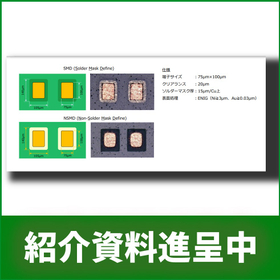
Technical Document on Solder Resist Formation Technology for Industrial Robots

We are offering materials that will assist in the design of high-precision industrial robot circuit boards!

In the industrial robot industry, the reliability of the circuit board is crucial for achieving high-precision movements. Particularly in circuit boards related to positioning and control, the accuracy of the solder resist significantly impacts the robot's performance. Defects in the solder resist can lead to malfunctions or failures, potentially resulting in decreased production efficiency. Our materials on solder resist formation technology include specifications such as terminal size, clearance, solder mask thickness, and surface treatment, which are helpful in product selection. 【Usage Scenarios】 - Robot arms requiring high-precision positioning - Robot hands performing delicate tasks - Industrial robots used in harsh environments 【Benefits of Implementation】 - Improved robot performance through optimized circuit board design - Reduced risk of failure by achieving reliable circuit boards - Shortened product selection time

Added to bookmarks

Bookmarks list

Bookmark has been removed

Bookmarks list

You can't add any more bookmarks

By registering as a member, you can increase the number of bookmarks you can save and organize them with labels.

Free membership registration

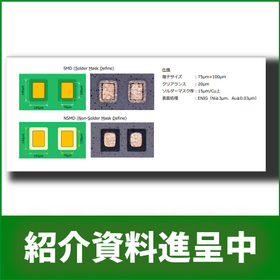
Aerospace Solder Resist Formation Technical Document

We present materials that include specifications such as terminal size, clearance, and solder mask thickness!

In the aerospace industry, there is a constant demand for lightweight products. In the design of printed circuit boards, solder resist significantly impacts component mounting density and reliability, making proper selection crucial. The selection of solder resist contributes to product miniaturization and weight reduction. Our materials on solder resist formation technology can help address these challenges. 【Application Scenarios】 - Electronics for aircraft and spacecraft - Circuit board designs requiring weight reduction - High-density mounting circuit boards 【Benefits of Implementation】 - Optimization of circuit board design - Weight reduction of products - Improved reliability

Added to bookmarks

Bookmarks list

Bookmark has been removed

Bookmarks list

You can't add any more bookmarks

By registering as a member, you can increase the number of bookmarks you can save and organize them with labels.

Free membership registration

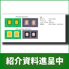
Technical Document on Solder Resist Formation for Smartphones

We present materials that are helpful for high-density smartphone circuit board design!

In the smartphone industry, high-density mounting of printed circuit boards is required due to miniaturization and increased functionality. It is particularly important to enhance the component placement density within limited space and ensure the reliability of electrical connections. Proper design of solder resist is essential for solving these challenges. Our materials on solder resist formation technology support the optimization of design for high-density mounting. 【Usage Scenarios】 - Design of high-density mounting boards - Optimization of component placement - Improvement of electrical connection reliability 【Effects of Implementation】 - Increased efficiency in board design - Miniaturization and high performance of products - Improved yield

Added to bookmarks

Bookmarks list

Bookmark has been removed

Bookmarks list

You can't add any more bookmarks

By registering as a member, you can increase the number of bookmarks you can save and organize them with labels.

Free membership registration

Technical Documentation for Solder Resist Formation for IoT Devices

Specifications such as terminal size, clearance, and solder mask thickness are listed.

In the IoT device industry, high durability that can withstand harsh environments is required. Especially for devices exposed to temperature changes, vibrations, and humidity, the reliability of printed circuit boards is a crucial factor that influences product lifespan. The proper selection and formation of solder resist are essential to protect the substrate from these external factors and ensure the long-term operation of the device. Our materials on solder resist formation technology will be helpful when selecting products. 【Usage Scenarios】 - Outdoor IoT devices - Industrial IoT equipment - IoT devices used in harsh environments 【Benefits of Implementation】 - Improved substrate protection performance - Enhanced product reliability - Assurance of long-term product lifespan

Added to bookmarks

Bookmarks list

Bookmark has been removed

Bookmarks list

You can't add any more bookmarks

By registering as a member, you can increase the number of bookmarks you can save and organize them with labels.

Free membership registration

Server-side solder resist formation technical documentation

Presentation of technical materials on solder resist technology that contributes to server acceleration.

In the server industry, there is a demand for improved data processing speeds and stability in signal transmission. Particularly, as high-density implementation progresses, the precision of solder resist becomes crucial. Inadequate solder resist can lead to signal interference and short circuits on the substrate, potentially resulting in a decline in server performance. Our materials on solder resist formation technology include specifications such as terminal size, clearance, and solder mask thickness, which are helpful in product selection. 【Usage Scenarios】 - Servers performing high-speed data communication - Servers using high-density implementation substrates - Servers where signal integrity is critical 【Benefits of Implementation】 - Stabilization of signal transmission - Improved reliability of the substrate - Reduction in product selection time

Added to bookmarks

Bookmarks list

Bookmark has been removed

Bookmarks list

You can't add any more bookmarks

By registering as a member, you can increase the number of bookmarks you can save and organize them with labels.

Free membership registration

Technical Document on Solder Resist Formation for Communication Infrastructure

Specifications such as terminal size, clearance, and solder mask thickness are listed.

In the telecommunications infrastructure industry, particularly in the field of signal integrity, the reliability of printed circuit boards is crucial. To ensure accurate signal transmission, precision in component placement on the board is required. Proper design and formation of solder resist prevent short circuits and disconnections, contributing to the long-term stability of the product. Our materials on solder resist formation technology are helpful during product selection. 【Usage Scenarios】 - PCB design for communication devices - Protection of signal transmission paths - Shielding of high-frequency circuits 【Benefits of Implementation】 - Improved board reliability - Increased product lifespan - Stabilization of signal quality

Added to bookmarks

Bookmarks list

Bookmark has been removed

Bookmarks list

You can't add any more bookmarks

By registering as a member, you can increase the number of bookmarks you can save and organize them with labels.

Free membership registration