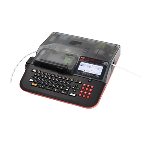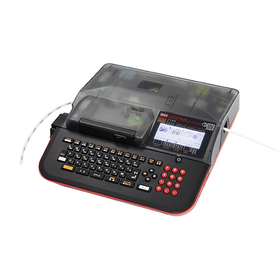
LM-500W3
Built-in tube warmer, PC link model
This is a portable tube marker for electrical equipment that can print on mark tubes and tape. ■ Main Features - Capable of printing on both thin and thick tubes, as well as tape. - Can operate cordlessly even in locations without power supply! (Compatible with rechargeable batteries (eneloop standard, AA x 4)). - High-speed printing at 40mm/second, capable of printing 52 mark tubes per minute! - Equipped with a tube warmer, ensuring safe operation even in cold winter conditions. - Easy creation of marking data with PC link function (download version)! *This product cannot print nameplates or device labels. If you wish to print nameplates or device labels, please check the page for "LM-550W3."
- Company:マックス
- Price:100,000 yen-500,000 yen