1~11 item / All 11 items
Displayed results

Added to bookmarks
Bookmarks listBookmark has been removed
Bookmarks listYou can't add any more bookmarks
By registering as a member, you can increase the number of bookmarks you can save and organize them with labels.
Free membership registration
Contact this company
Inquiry FormBefore making an inquiry
Download Profile1~11 item / All 11 items
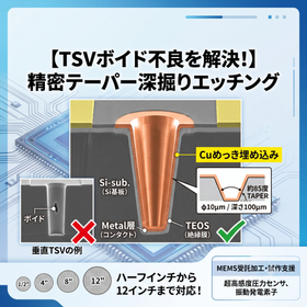
M.T.C Corporation is a research and development-oriented contract processing company with the corporate philosophy of "bridging the seeds and needs of MEMS technology." We aim to contribute to society through "environmentally friendly technology" such as miniaturization and integration. Are you facing issues such as void formation during Cu plating embedding, contact failures due to bottom breakage or residues, and the absence of seed sputter film on the via bottom side in the TSV (Through-Silicon Via) formation process? Our company provides a solution that fundamentally addresses these challenges by intentionally establishing a taper angle during the deep etching stage. Furthermore, we strongly support not only processing but also the advanced development of MEMS devices, such as vibration energy harvesting elements for next-generation IoT devices.
Added to bookmarks
Bookmarks listBookmark has been removed
Bookmarks listYou can't add any more bookmarks
By registering as a member, you can increase the number of bookmarks you can save and organize them with labels.
Free membership registration
We would like to introduce the processing contract services offered by M.T.C Corporation. With our extensive knowledge and experience gained from semiconductor processing, we provide MEMS contract processing services, including anodic bonding, metal-metal bonding, and plasma activation bonding in the bonding process. Additionally, we perform pre-treatment, film deposition, photolithography, etching, and electroplating. Please feel free to contact us if you have any requests. 【Processing Details】 ■ Pre-treatment ■ Film Deposition ■ Photolithography ■ Etching ■ Electroplating ■ Bonding *For more details, please download the PDF or feel free to contact us.
Added to bookmarks
Bookmarks listBookmark has been removed
Bookmarks listYou can't add any more bookmarks
By registering as a member, you can increase the number of bookmarks you can save and organize them with labels.
Free membership registration
We would like to introduce the processing contract services offered by M.T.C Corporation. With the extensive knowledge and experience gained from semiconductor processing, we provide MEMS contract processing services, including Cu plating, Ni plating, and Au plating through electroplating. Additionally, we also perform pre-treatment, film formation, photolithography, etching, and bonding. Please feel free to contact us if you have any requests. 【Processing Details】 ■ Pre-treatment ■ Film formation ■ Photolithography ■ Etching ■ Electroplating ■ Bonding *For more details, please download the PDF or feel free to contact us.
Added to bookmarks
Bookmarks listBookmark has been removed
Bookmarks listYou can't add any more bookmarks
By registering as a member, you can increase the number of bookmarks you can save and organize them with labels.
Free membership registration
We would like to introduce the processing contract services offered by M.T.C Corporation. With the extensive knowledge and experience gained from semiconductor processing, we provide MEMS contract processing services, including Wet etching, Dry etching, and DRIE in the etching process. Additionally, we also perform pre-treatment, film formation, photolithography, electroplating, and bonding. Please feel free to contact us if you have any requests. 【Processing Details】 ■ Pre-treatment ■ Film Formation ■ Photolithography ■ Etching ■ Electroplating ■ Bonding *For more details, please download the PDF or feel free to contact us.
Added to bookmarks
Bookmarks listBookmark has been removed
Bookmarks listYou can't add any more bookmarks
By registering as a member, you can increase the number of bookmarks you can save and organize them with labels.
Free membership registration
We would like to introduce the processing contract services offered by M.T.C Corporation. With the extensive knowledge and experience gained from semiconductor processing, we provide MEMS contract processing services, including photolithography using contact aligners, steppers, and EB lithography. Additionally, we also perform pre-treatment, film formation, etching, electroplating, and bonding. Please feel free to contact us if you have any requests. 【Processing Details】 ■ Pre-treatment ■ Film formation ■ Photolithography ■ Etching ■ Electroplating ■ Bonding *For more details, please download the PDF or feel free to contact us.
Added to bookmarks
Bookmarks listBookmark has been removed
Bookmarks listYou can't add any more bookmarks
By registering as a member, you can increase the number of bookmarks you can save and organize them with labels.
Free membership registration
We would like to introduce the processing contract services offered by M.T.C. Corporation. Our company provides MEMS contract processing services with extensive knowledge and experience gained from semiconductor processing. In the film deposition process, we carry out thermal Si oxidation deposition, CVD deposition, and metal deposition. Additionally, we also perform pre-treatment, photolithography, etching, electroplating, and bonding. Please feel free to contact us if you have any requests. 【Processing Details】 ■ Thermal Si Oxidation Deposition ■ CVD Deposition ・SiO2, SiN ■ Metal Deposition ・Al, Al-Si, Al-Cu, Cu, Ti, W, Mo *For more details, please download the PDF or feel free to contact us.
Added to bookmarks
Bookmarks listBookmark has been removed
Bookmarks listYou can't add any more bookmarks
By registering as a member, you can increase the number of bookmarks you can save and organize them with labels.
Free membership registration
We would like to introduce the processing contract services offered by M.T.C Corporation. With our extensive knowledge and experience gained from semiconductor processing, we provide MEMS contract processing services, and we offer RCA cleaning in the pre-treatment process. Additionally, we also perform film deposition, photolithography, etching, electroplating, and bonding. Please feel free to contact us if you have any requests. 【Processing Details】 ■ Pre-treatment ■ Film deposition ■ Photolithography ■ Etching ■ Electroplating ■ Bonding *For more details, please download the PDF or feel free to contact us.
Added to bookmarks
Bookmarks listBookmark has been removed
Bookmarks listYou can't add any more bookmarks
By registering as a member, you can increase the number of bookmarks you can save and organize them with labels.
Free membership registration
Our company is engaged in energy harvesting operations, including the development of vibration power generation elements using magnetostrictive thin films to solve the "power supply problem" of IoT. In the NEDO New Energy Venture Technology Innovation Project Stage B, we have made improvements such as generating power at 30Hz and 0.15G acceleration, and laminating magnetostrictive thin films, achieving the target value of 50μW. We also offer technical consulting related to MEMS and assistance in business startups. Please feel free to contact us if you have any requests. 【Business Contents】 ■ Energy Harvesting ■ Technical Consulting *For more details, please download the PDF or feel free to contact us.
Added to bookmarks
Bookmarks listBookmark has been removed
Bookmarks listYou can't add any more bookmarks
By registering as a member, you can increase the number of bookmarks you can save and organize them with labels.
Free membership registration
Our company is engaged in the development of various MEMS devices, multi-sensor data loggers, and sensor network products. We are developing ultra-high sensitivity pressure sensors and implementing TSV processing such as tapered etching and scallop-free (minimal fab). Additionally, we are involved in the development of microelectronic components using thick-film plating. Please feel free to contact us if you have any requests. 【Business Activities】 ■ Development of ultra-high sensitivity pressure sensors ■ TSV processing: tapered etching, scallop-free (minimal fab) ■ Development of microelectronic components using thick-film plating, etc. *For more details, please download the PDF or feel free to contact us.
Added to bookmarks
Bookmarks listBookmark has been removed
Bookmarks listYou can't add any more bookmarks
By registering as a member, you can increase the number of bookmarks you can save and organize them with labels.
Free membership registration
M.T.C Corporation provides various MEMS processing contract services, including EB exposure, DRIE, and anodic bonding. We carry out processing of development products, Si deep etching, and various film deposition processes, ranging from 0.5 inch to 12 inch. Our company acts as a bridge between the seeds and needs of MEMS technology. We invite you to utilize our services for the development of your MEMS-related business. 【Business Contents】 ■ Processing of development products ■ Si deep etching ■ Various film deposition *For more details, please download the PDF or feel free to contact us.
Added to bookmarks
Bookmarks listBookmark has been removed
Bookmarks listYou can't add any more bookmarks
By registering as a member, you can increase the number of bookmarks you can save and organize them with labels.
Free membership registration
Our company offers a variety of MEMS (Micro Electro Mechanical Systems) processing services, including EB lithography, DRIE, and anodic bonding, based on our extensive knowledge and experience gained from semiconductor processing. We provide a wide range of services, including development product processing, elemental technology processing, deep silicon etching, and various film deposition. Additionally, we are also engaged in minimal fab. You can check the important issues regarding process technology in TSV formation through PDF downloads. 【Processing Details】 ■ Pre-treatment (RCA cleaning) ■ Film deposition (thermal Si oxidation film, CVD deposition [SiO2, SiN], metal deposition [Al, Al-Si, Al-Cu, Cu, Ti, W, Mo]) ■ Photolithography (contact aligner, stepper, EB lithography) ■ Etching (wet etching, dry etching, DRIE) ■ Electrodeposition (Cu plating, Ni plating, Au plating) ■ Bonding (anodic bonding, metal-metal bonding, plasma activated bonding) *For more details, please download the PDF or feel free to contact us.
Added to bookmarks
Bookmarks listBookmark has been removed
Bookmarks listYou can't add any more bookmarks
By registering as a member, you can increase the number of bookmarks you can save and organize them with labels.
Free membership registration