September 17 Webinar Announcement: Surface Treatment and Packaging Technologies Supporting Semiconductors in the AI Era - Why is "Connecting Technology" Gaining Attention Now?
 メルテックス
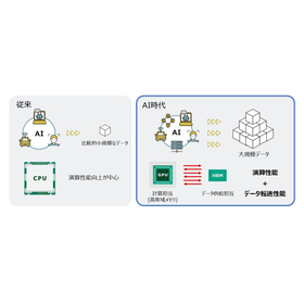
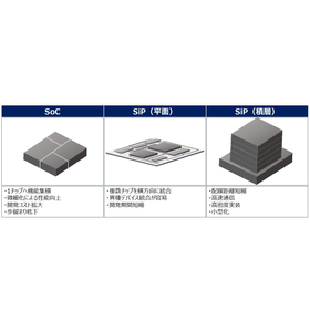
With the spread of AI, semiconductors are being demanded to have higher speeds and larger capacities than ever before. On the other hand, the miniaturization that has supported performance improvements is beginning to show its limits. In this context, attention is being drawn to implementation technologies that combine multiple chips to enhance performance. With the spread of HBM and chiplets, the focus of competition in the semiconductor industry is shifting from "the technology to make chips" to "the technology to connect chips." This seminar will explain the background of why implementation technology is becoming important in the AI era, as well as introduce recent trends in middle-process and connection structure technologies. Additionally, it will clearly explain the role of plating and surface treatment technologies that support these advancements. This seminar aims to provide information that will lead the semiconductor business in the AI era for those who want to grasp industry trends and implementation technology trends.
Date: September 17, 2026 (Thursday)
Time: 11:00 AM - 11:50 AM (Japan Time)
Cost: Free
Instructor: Takahiro Shimoda, Sales Department, Japan Sales Group, Western Japan Sales Division
Format: Webinar (Zoom)
Inquiry about this news
Contact Us OnlineMore Details & Registration
Details & Registration
Related Links
Please register using the application form at the link.
Distributors