iPROS Manufacturing
  • Search for products by classification category

    • Electronic Components and Modules
      Electronic Components and Modules
      59878items
    • Machinery Parts
      Machinery Parts
      74899items
    • Manufacturing and processing machinery
      Manufacturing and processing machinery
      100569items
    • Scientific and Physics Equipment
      Scientific and Physics Equipment
      35539items
    • Materials
      Materials
      37274items
    • Measurement and Analysis
      Measurement and Analysis
      55137items
    • Image Processing
      Image Processing
      15219items
    • Control and Electrical Equipment
      Control and Electrical Equipment
      53515items
    • Tools, consumables, and supplies
      Tools, consumables, and supplies
      64612items
    • Design and production support
      Design and production support
      12473items
    • IT/Network
      IT/Network
      44136items
    • Office
      Office
      13849items
    • Business support services
      Business support services
      24474items
    • Seminars and Skill Development
      Seminars and Skill Development
      6417items
    • Pharmaceutical and food related
      Pharmaceutical and food related
      31366items
    • others
      74231items
  • Search for companies by industry

    • Manufacturing and processing contract
      7336
    • others
      5009
    • Industrial Machinery
      4411
    • Machine elements and parts
      3282
    • Other manufacturing
      2881
    • IT/Telecommunications
      2556
    • Trading company/Wholesale
      2472
    • Industrial Electrical Equipment
      2301
    • Building materials, supplies and fixtures
      1815
    • software
      1632
    • Electronic Components and Semiconductors
      1566
    • Resin/Plastic
      1493
    • Service Industry
      1450
    • Testing, Analysis and Measurement
      1127
    • Ferrous/Non-ferrous metals
      981
    • environment
      697
    • Chemical
      628
    • Automobiles and Transportation Equipment
      560
    • Printing Industry
      508
    • Information and Communications
      455
    • Consumer Electronics
      417
    • Energy
      329
    • Rubber products
      312
    • Food Machinery
      306
    • Optical Instruments
      276
    • robot
      272
    • fiber
      250
    • Paper and pulp
      229
    • Pharmaceuticals and Biotechnology
      167
    • Electricity, Gas and Water Industry
      167
    • Warehousing and transport related industries
      146
    • Glass and clay products
      140
    • Food and Beverage
      128
    • CAD/CAM
      123
    • retail
      109
    • Medical Devices
      103
    • Educational and Research Institutions
      102
    • Ceramics
      98
    • wood
      88
    • Transportation
      82
    • Petroleum and coal products
      62
    • Medical and Welfare
      62
    • Shipbuilding and heavy machinery
      51
    • Aviation & Aerospace
      48
    • Fisheries, Agriculture and Forestry
      41
    • equipment
      32
    • Public interest/special/independent administrative agency
      31
    • Materials
      25
    • self-employed
      24
    • Research and development equipment and devices
      24
    • Government
      23
    • Mining
      17
    • Finance, securities and insurance
      13
    • cosmetics
      12
    • Individual
      10
    • Restaurants and accommodations
      9
    • Police, Fire Department, Self-Defense Forces
      7
    • Raw materials for reagents and chemicals
      3
    • Laboratory Equipment and Consumables
      3
    • Contracted research
      3
  • Special Features
  • Ranking

    • Overall Products Ranking
    • Overall Company Ranking
Search for Products
  • Search for products by classification category

  • Electronic Components and Modules
  • Machinery Parts
  • Manufacturing and processing machinery
  • Scientific and Physics Equipment
  • Materials
  • Measurement and Analysis
  • Image Processing
  • Control and Electrical Equipment
  • Tools, consumables, and supplies
  • Design and production support
  • IT/Network
  • Office
  • Business support services
  • Seminars and Skill Development
  • Pharmaceutical and food related
  • others
Search for Companies
  • Search for companies by industry

  • Manufacturing and processing contract
  • others
  • Industrial Machinery
  • Machine elements and parts
  • Other manufacturing
  • IT/Telecommunications
  • Trading company/Wholesale
  • Industrial Electrical Equipment
  • Building materials, supplies and fixtures
  • software
  • Electronic Components and Semiconductors
  • Resin/Plastic
  • Service Industry
  • Testing, Analysis and Measurement
  • Ferrous/Non-ferrous metals
  • environment
  • Chemical
  • Automobiles and Transportation Equipment
  • Printing Industry
  • Information and Communications
  • Consumer Electronics
  • Energy
  • Rubber products
  • Food Machinery
  • Optical Instruments
  • robot
  • fiber
  • Paper and pulp
  • Pharmaceuticals and Biotechnology
  • Electricity, Gas and Water Industry
  • Warehousing and transport related industries
  • Glass and clay products
  • Food and Beverage
  • CAD/CAM
  • retail
  • Medical Devices
  • Educational and Research Institutions
  • Ceramics
  • wood
  • Transportation
  • Petroleum and coal products
  • Medical and Welfare
  • Shipbuilding and heavy machinery
  • Aviation & Aerospace
  • Fisheries, Agriculture and Forestry
  • equipment
  • Public interest/special/independent administrative agency
  • Materials
  • self-employed
  • Research and development equipment and devices
  • Government
  • Mining
  • Finance, securities and insurance
  • cosmetics
  • Individual
  • Restaurants and accommodations
  • Police, Fire Department, Self-Defense Forces
  • Raw materials for reagents and chemicals
  • Laboratory Equipment and Consumables
  • Contracted research
Special Features
Ranking
  • Overall Products Ranking
  • Overall Company Ranking
  • privacy policy
  • terms of service
  • About Us
  • Careers
  • Advertising
  1. Home
  2. ProductSearch
  3. Scientific and Physics Equipment
  4. Surface Treatment Equipment
  5. Surface treatment contract service
  6. Contract processing of analytical chips for electrochemical measurements: Calculating dielectric constant from the desired capacitance.

Contract processing of analytical chips for electrochemical measurements: Calculating dielectric constant from the desired capacitance.

  • Added to bookmarks

    Bookmarks list

    Bookmark has been removed

    Bookmarks list

    You can't add any more bookmarks

    By registering as a member, you can increase the number of bookmarks you can save and organize them with labels.

    Free membership registration

last updated:Dec 24, 2024

安達新産業 本社
安達新産業 本社
  • Official site

We offer contract processing for analytical chips for electrochemical (bio) measurements.

Are you facing any of these issues? - It's difficult to manage delivery times when ordering thin film processing and pattern processing separately. - I haven't put it into a drawing, but can you provide consultation? - I want to achieve fine wiring, but I would like advice on film materials. - Can you accept just pattern processing? - Can you handle line and space (L/S) down to 10μm? 1) We realize fine pattern processing. We achieve fine patterning through photolithography, etching, and metal masks. We select the best processing method and resist according to the customer's requirements. 2) We can provide integrated production from substrate procurement to film formation. At Adachi New Industry, we can respond to custom orders consistently from substrate procurement to film processing, fine processing, and chip processing. It is also possible to cut into any shape and ship as components. However, we need detailed drawings, etc. 3) We accommodate cleanroom requirements. The working environment maintains the necessary cleanliness for each stage from film formation to inspection, and we have a thorough system in place to address minor film defects (such as foreign substances in the film).

    Surface treatment contract service
denki_tip.jpg

Contract processing of analytical chips for electrochemical measurements: Calculating dielectric constant from the desired capacitance.

denki_tip.jpg
denki_tip.jpg
  • Related Link - https://www.e-coating.jp/solutions/pattern/lineup1…

Inquire About This Product

  • Contact Us Online
  • Download catalog

basic information

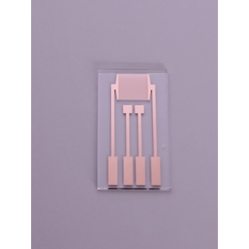
【1】Processing Accuracy ● Electrode Line Width: Several μm ● Electrode Spacing: Several μm (Please consult us for sub-μm and nm level patterns.) 【2】Electrode Materials ● Au, Pt, Ag, C, ITO, DLC, alloys, etc. ● Organic films, insulating films, etc. ● Selective permeable films, etc. ● Multilayer electrodes of dissimilar metals and alloys 【3】Small-scale prototyping is also possible. In manufacturing, the cycle of hypothesis and verification is an essential process. No matter how advanced simulation technology becomes, verification cannot be omitted. Therefore, at Adachi New Industry, we are happy to undertake prototyping for characteristic verification. Please contact us first. *All products are custom-made, and we accept orders with a consistent system from electrode configuration, drawing creation, to chip processing.

Price information

The price will vary depending on the pattern shape and quantity. Please feel free to contact us first. We would appreciate it if you could provide the following information at the same time to ensure a smooth proposal: - Purpose - Information about the metal film: number of layers, thickness - Substrate information: glass, resin, Si wafer, SiC wafer, etc. - Product size, thickness - Pattern drawing - Final product (as much information as you can share).

Delivery Time

P4

Applications/Examples of results

● Electrochemical analysis, organic semiconductor analysis electrodes ● Bioscience, organic electronics ● Electrodes for various sensors (gas sensors, etc.) ● Electrodes for SOFC (solid oxide fuel cell) materials ● Others, special fine electrodes, etc.

catalog(3)

Download All Catalogs
Electrochemical analysis chip contract manufacturing Adachi New Industry Co., Ltd.

Electrochemical analysis chip contract manufacturing Adachi New Industry Co., Ltd.

PRODUCT
  • E-book viewing
  • Catalog download

Contact this catalog

Pattern processing_photolithography_etching Adachi New Industry Co., Ltd.

Pattern processing_photolithography_etching Adachi New Industry Co., Ltd.

PRODUCT
  • E-book viewing
  • Catalog download

Contact this catalog

Metalized Pattern Processing Adachi New Industry Co., Ltd.

Metalized Pattern Processing Adachi New Industry Co., Ltd.

PRODUCT
  • E-book viewing
  • Catalog download

Contact this catalog

News about this product(33)

Co-creation proposal! Added 'Agriculture × Optical Films' as a technology trend keyword.

  • Company news

In recent years, technological innovations in the agricultural sector have significantly shifted from traditional biological approaches such as soil improvement and breeding to an engineering concept of "designing the environment itself." Particularly noteworthy is smart agriculture, which integrates precise control of light environments with sensing technology. Plant growth is complexly determined not only by light intensity but also by wavelength distribution, angle of incidence, temporal variations, and interactions with surrounding temperatures. In other words, agriculture can essentially be described as "the science of spectral control." In this context, optical thin films and optical filters play an extremely important role. Optical thin films are functional materials that allow for precise design of reflectivity, transmittance, absorbance, and interference characteristics through control of film thickness on the nanometer scale. By using multilayer interference structures, it is possible to selectively transmit and reflect specific wavelengths, which directly contributes to optimizing effective light for photosynthesis in plants and controlling unwanted infrared and ultraviolet light. For more information, please check our company website.

Added to bookmarks

Bookmarks list

Bookmark has been removed

Bookmarks list

You can't add any more bookmarks

By registering as a member, you can increase the number of bookmarks you can save and organize them with labels.

Free membership registration

Added to the technology trend keywords: 'Why thin film metallization is necessary for electrochemical analysis chips in 5 minutes!'

  • Company news

Electrochemical analysis chips are devices that utilize electrical signals such as voltage and current to read chemical reactions. The chip is equipped with working electrodes, counter electrodes, and reference electrodes, allowing for the highly sensitive detection of redox reactions occurring in solution. In recent years, compact devices combining microfluidic technology and MEMS technology have become widespread, rapidly expanding their use in medical POCT (Point of Care Testing), environmental monitoring, food testing, and life sciences. In these applications, there is a demand for higher sensitivity, miniaturization, multiplexing, and speed of detection, and essential to achieving this are the miniaturization of electrode structures and the formation of high-quality metal thin films, namely thin film metallization technology. ◆ Key to electrochemical analysis: The quality of data is determined by the performance of the electrodes ◆ Thus, "thin film metallization" is necessary ◆ Technical points when performing thin film metallization ◆ Examples of performance improvements brought by thin film metallization ◆ Future trends: Demand accelerating with POCT and wearables ◆ The inseparable relationship between electrochemical analysis chips and thin film technology For more details, please check our company website.

Added to bookmarks

Bookmarks list

Bookmark has been removed

Bookmarks list

You can't add any more bookmarks

By registering as a member, you can increase the number of bookmarks you can save and organize them with labels.

Free membership registration

Added 'Flexible Devices and Sputtering' to the technology trend keywords.

  • Product news

In recent years, the evolution of electronic devices has garnered significant attention for flexible devices. These devices leverage their ability to be bent and stretched, with applications expected in various fields such as wearable devices, next-generation displays, and medical equipment. One of the key technologies supporting this realization is "sputtering." Sputtering excels in the precision and diversity of thin film formation, making it possible to create layers with advanced functions on flexible substrates. This document describes the role of sputtering technology in flexible devices and examples of its applications. 1. What are flexible devices 2. Main application areas 3. Key points for forming sputtered thin films suitable for flexible devices For more details, please check our company website.

Added to bookmarks

Bookmarks list

Bookmark has been removed

Bookmarks list

You can't add any more bookmarks

By registering as a member, you can increase the number of bookmarks you can save and organize them with labels.

Free membership registration

I added 'TEG chips for SiC' to the technical trend keywords.

  • Company news

In semiconductor manufacturing, TEG (Test Element Group) chips are essential for evaluating the accuracy and stability of processes. To detect subtle variations in the manufacturing line and improve yield, extremely high technology is required for the metallization (wiring formation) and patterning on TEG chips. In particular, SiC power devices are characterized by high voltage resistance, high-temperature operation, and high-frequency operation, and they exhibit different failure modes and mechanisms compared to silicon (such as breakdown under high electric fields, interface traps, and degradation originating from grain boundaries). Therefore, a TEG specifically for the SiC process is necessary. 【1】What is a TEG chip? - Purpose and Importance 【2】Key Technical Challenges in SiC Processing (Considerations during TEG Fabrication) 【3】Metallization Technology 【4】Patterning Technology 【5】Cross-Impact of SiC Device Technology and Market Summary For more details, please visit our website.

Added to bookmarks

Bookmarks list

Bookmark has been removed

Bookmarks list

You can't add any more bookmarks

By registering as a member, you can increase the number of bookmarks you can save and organize them with labels.

Free membership registration

Companynews list (168)

Company information

安達新産業

安達新産業 本社

Optical Instruments

Added to bookmarks

Bookmarks list

Bookmark has been removed

Bookmarks list

You can't add any more bookmarks

By registering as a member, you can increase the number of bookmarks you can save and organize them with labels.

Free membership registration
  • Official site
Phone number/address

Since our founding in Taisho 8 (1919), we have cultivated an extensive network as a chemical industrial trading company and will respond to all of our customers' needs through various surface treatment technologies, including optical thin film processing (optical coating). Company Name: Adachi Shinsangyo Co., Ltd. Representative Director: Kensuke Adachi Capital: 10 million yen Founded: November, Taisho 7 (1918) Established: August, Showa 39 (1964) Location: ■ Head Office: 10F Anix Building, 1-14-20 Tachiuri-bori, Nishi-ku, Osaka 550-0012 Phone: 06-6536-2051 / FAX: 06-6536-2015 ■ Higashi-Osaka Factory: 3-3-1 Tamakushicho Higashi, Higashi-Osaka City 578-0932 Phone: 072-962-4133 / FAX: 072-964-9055 Group Companies: Osaka Vacuum Industry Co., Ltd., Adachi Kousan Co., Ltd.

Product/Service List (35)

Related Popular Products

Structural calculation (allowable stress calculation) / wall quantity calculation (frame calculation)
others
Structural calculation (allowable stress calculation) / wall quantity calculation (frame calculation)
在住ビジネス 本社
FANDX Application Estimate Calculation
IT/Network
FANDX Application Estimate Calculation
豆蔵
Principles of Flatness Calculation for 3D Printing
others
Principles of Flatness Calculation for 3D Printing
松井製作所
Foundation, Pile, and Ground Series Calculation BUS - Foundation Structure
Design and production support
Foundation, Pile, and Ground Series Calculation BUS - Foundation Structure
構造システム・グループ
Calculation of the properties of optical thin film coatings "TFCalc"
Measurement and Analysis
Calculation of the properties of optical thin film coatings "TFCalc"
ヒューリンクス

Related New Products

Measures to prevent liquid from creeping up the dispenser.
Scientific and Physics Equipment
Measures to prevent liquid from creeping up the dispenser.
日建塗装工業
Coating for hot rivet resin adhesion and thread pulling prevention.
Scientific and Physics Equipment
Coating for hot rivet resin adhesion and thread pulling prevention.
日建塗装工業
PFAS regulation compliance! Ceramic-based non-stick coating for food applications.
Scientific and Physics Equipment
PFAS regulation compliance! Ceramic-based non-stick coating for food applications.
日建塗装工業
Improving the yield of label printing: Measures against adhesive troubles.
Scientific and Physics Equipment
Improving the yield of label printing: Measures against adhesive troubles.
日建塗装工業
Selecting Surface Treatments Without Failing in PFAS-Free Solutions
Scientific and Physics Equipment
Selecting Surface Treatments Without Failing in PFAS-Free Solutions
日建塗装工業

The related categories of Surface treatment contract service

  • Scientific and Physics Equipment
  • Surface Treatment Equipment
  • Surface treatment contract service
Find products and companies by related keywords
  • #Calculation
  • #Rate Calculation
          

Inquire About This Product

  • Contact Us Online
  • Download catalog

Products

  • Search for Products

Company

  • Search for Companies

Special Features

  • Special Features

Ranking

  • Overall Products Ranking
  • Overall Company Ranking

support

  • site map
IPROS
  • privacy policy Regarding external transmission of information
  • terms of service
  • About Us
  • Careers
  • Advertising
COPYRIGHT © 2001-2026 IPROS CORPORATION ALL RIGHTS RESERVED.
Please note that the English text on this page is automatically translated and may contain inaccuracies.