High etching effect regardless of organic or inorganic! Rental starts from one week♪ Easy to use with touch panel control.
Contract etching of Si and carbon films! In addition, it can be used for various applications such as the fabrication of fine circuits like semiconductor integrated circuits. Available for rental for one week or more to support research and development quickly! Initial condition proposals and demo processing are provided free of charge.

Inquire About This Product
basic information
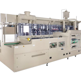
Output: MAX300W Frequency: 13.56MHz Dimensions: 510(W) × 850(H) × 760(D) mm Weight: Approximately 85Kg Gas System: One mass flow controller (two systems are optional) Float-type flow meter Stage Dimensions: φ200mm Power Supply: AC100V 50/60Hz 15A Vacuum Pump: 135/160 (liters/min) Operation Method: Automatic operation via touch panel
Price range
Delivery Time
Applications/Examples of results
【Surface Modification】 ☆Content - Surface modification / Dry cleaning / Improvement of hydrophilicity / Enhancement of adhesion effects / Pre-treatment for printing and painting / Removal of organic substances / Improvement of wettability / Cell culture, etc... ☆Materials Metals, glass, resins, powders, tubes, etc. 【Etching】 ☆Content - Contract processing of dry etching (silicon, glass, metal) 【Film Formation】 ☆Content - Formation of SiO2 films and TEOS films 【Examples】 ☆Content - Cleaning of glass and pre-treatment for adhesion - Cleaning of LSI and pre-treatment for adhesion - Cleaning of resin molded products and pre-treatment for adhesion - Substrate cleaning for solar cells and fuel cells - Terminal cleaning for organic EL, digital signage-related displays, and LCD substrates - Pre-treatment for wire bonding - Cleaning of films and pre-treatment for adhesion - Cleaning of MEMS, etc. - Pre-cleaning before plating - Pre-treatment for printing on paper - Cleaning of semiconductor wafers - Cleaning of silicon wafers, etc...
catalog(6)
Download All Catalogs![PEN-type atmospheric pressure plasma [340,000]](https://image.mono.ipros.com/public/catalog/image_generated/01/736/10852/10852_IPROS7147937134213498867_1.jpg?w=120&h=170)
![Yes, SiO2 Plasma Etcher [CPE-300S]](https://image.mono.ipros.com/public/catalog/image/01/b19/284895/IPROS2658882672484167289.png?w=120&h=170)


![Tabletop vacuum plasma device [490,000 yen]](https://image.mono.ipros.com/public/catalog/image_generated/01/098/272265/272265_IPROS7964277887727693311_1.jpg?w=120&h=170)

Company information

KAI Semiconductor was established in September 2002 as a venture company originating from Kyoto Institute of Technology. It sells surface modification devices and deposition equipment using plasma technology. The powder plasma device released in 2010 was recognized for its high technical capabilities and received the "Kansai Front Runner Award" and the "Small and Medium Enterprises Technology Award." There are numerous implementation records at universities nationwide, AIST, major manufacturers, and R&D departments. We propose sales after you have had the opportunity to touch the actual product (demo unit). Additionally, we offer rental and leasing options to reduce the burden on our customers. We also accept various technical consultations beyond semiconductor-related matters. Furthermore, we process and sell quartz and Pyrex in small lots.
![Plasma Etcher Semi-Auto Series [CPE-300S]](https://image.mono.ipros.com/public/product/image/a5c/2000369160/IPROS10036028945008327953.png?w=280&h=280)

![[Research Material] Global Market for Wafer Etchers](https://image.mono.ipros.com/public/product/image/400/2001473351/IPROS46570483328554376370.jpeg?w=280&h=280)
![[Tooling-Free Mass Production] Machined Production Parts](https://image.mono.ipros.com/public/product/image/2000158412/IPROS4317513488585082420.JPG?w=280&h=280)